General Documentation:
Inertial Delay
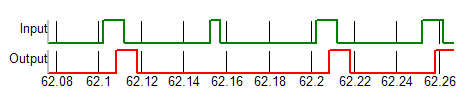
Any Input to Output delay for the new Advanced Digital components incorporates inertial delay where, if the pulse width of the incoming signal is less than the Input to Output delay of a particular device, then there is no resulting change in the output. In the example below, one of the input pulses is narrower than the input-to-output delay of a buffer logic gate. In that instance, the output of the buffer gate effectively "ignores" that one input pulse.
This inertial delay behavior describes the Delay parameter for all the Advanced Digital Logic Gates as well as the Out Delay of the Adder, Subtracter, Multiplier, Comparator and Latches and each of the delay parameters of the Analog-to-Digital Converters, Counters and Flip Flops.
None of the delay parameters of the SIMPLIS Advanced Digital components may be set to zero.
Transport Delay
By contrast, the Classic SIMPLIS digital gates model transport delay, in which they are able to respond to any width signal at their input and reproduce that same width signal at the output after the specified delay interval.
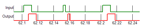
The Classic Digital components may have their delay parameters set to zero.
Flip-Flop Delay Parameters
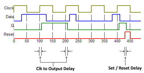
This example shows an edge triggered D-type flip flop with asynchronous set and reset. In this example, Set and Reset are selected to be active high. The following diagram shows the definition of the Clk to Output Delay as well as the Set/Reset Delay. All Flip Flop devices have a Clk to Output Delay parameter and all Flip Flops with the Set and Reset feature have a Set/Reset Delay.
Flip-Flop Minimum Clock Width
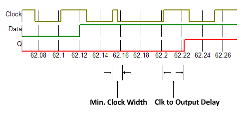
As in this example of a D-type flip flop, where the device is set to trigger on the positive going edge of the clock, if the width of the clock pulse is narrower than the specified Minimum Clock Width, the clock pulse is ignored.
Discrete Filters
Device Operation:
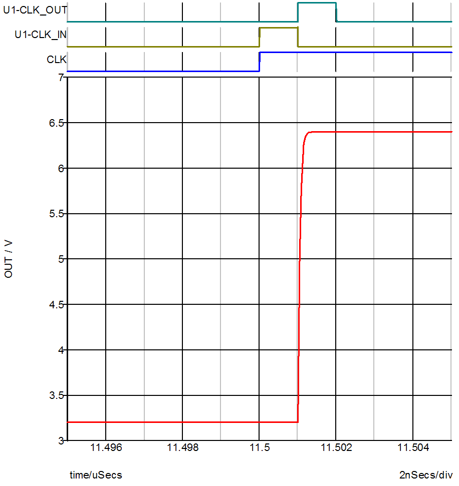
Each of these discrete filters is driven by an input clock signal. For proper operation, the input clock signal needs to be made up of a train of pulses with pulse widths equal to or wider than the "Time of Acquisition" set for the filter. For the most efficient simulation, this kind of pulses can be generated by driving periodic pulses through the "Sampling Clock Generator for Discrete Filters." If the "Sampling Clock Generator for Discrete Filters" is used to generate the input clock signals for the discrete filters, the driving periodic pulses can have pulse widths shorter than the time of acquisition as long as they are well defined pulses.
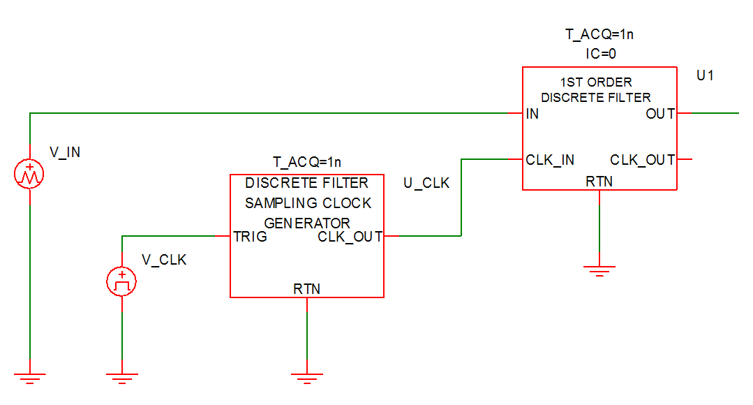
If the time of acquisition is tACQ, then the "Sampling Clock Generator for Discrete Filters" will generate a pulse whose pulse width is equal to tACQ every time its "TRIG" input makes a positive transition exceeding 3V. During this pulse, the discrete filter will sample the input data at the "IN" input pin and it will take tACQ for it to satisfactorily acquire the input data. After tACQ has expired, the discrete filter will update its output, and the output will settle within a time duration less than or equal to tACQ. In addition, during this duration when the output is updated, the output "CLK_OUT" is raised to a high value.
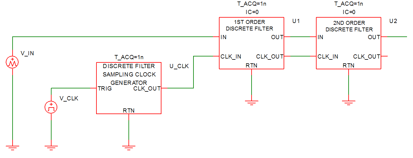
A discrete filter with more than two poles can be synthesized through a cascade of one-pole and/or two-pole discrete filters. In such case, the timing signal for each driven stage is derived from the "CLK_OUT" signal of the immediately preceding stage.
Flip-Flops:
D-Type Flip-Flop |
D-Type Flip-Flop w/ SET/RST |
S/R Flip-Flop |
S/R Flip-Flop w/ SET/RST |
J/K Flip-Flop |
J/K Flip-Flop w/ SET/RST |
Toggle Flip-Flop |
Toggle Flip-Flop w/ SET/RST |
top![]()
D-Type Flip-Flop
Clk to Output Delay
| Property Name: | CLK_TO_OUT_DELAY (Additional Info) |
|---|---|
| Data Type: | NUMBER |
| Description: | Delay from triggering edge of clock until output changes |
Ground Ref
| Property Name: | GNDREF |
|---|---|
| Data Type: | STRING |
| Options: | Y, N |
| Description: | Determines whether or not a device has a ground reference pin |
Hold Time
| Property Name: | HOLD_TIME |
|---|---|
| Data Type: | NUMBER |
| Description: | Minimum time that input data signals must remain constant after triggering clock edge to register as a valid change in input state |
Hysteresis
| Property Name: | HYSTWD |
|---|---|
| Data Type: | NUMBER |
| Description: | Hysteretic-window width centered around TH (Threshold voltage) |
Initial Condition
| Property Name: | IC |
|---|---|
| Data Type: | NUMBER |
| Options: | 0, 1 |
| Description: | Initial condition of the flip-flop's output |
Minimum Clk Width
| Property Name: | MIN_CLK (Additional Info) |
|---|---|
| Data Type: | NUMBER |
| Description: | Minimum valid clock width |
Input Resistance
| Property Name: | RIN |
|---|---|
| Data Type: | NUMBER |
| Description: | Input resistance |
Output Resistance
| Property Name: | ROUT |
|---|---|
| Data Type: | NUMBER |
| Description: | Output resistance |
Setup Time
| Property Name: | SETUP_TIME |
|---|---|
| Data Type: | NUMBER |
| Description: | Minimum time that input data signals must remain constant before triggering clock edge to register as a valid change in input state |
Threshold
| Property Name: | TH |
|---|---|
| Data Type: | NUMBER |
| Description: | Threshold voltage |
Trigger Condition
| Property Name: | TRIG_COND |
|---|---|
| Data Type: | STRING |
| Options: | 0_TO_1, 1_TO_0 |
| Description: | Determines the triggering condition of the clock pin, either the rising edge or the falling edge |
Output High Voltage
| Property Name: | VOH |
|---|---|
| Data Type: | NUMBER |
| Description: | Output high voltage |
Output Low Voltage
| Property Name: | VOL |
|---|---|
| Data Type: | NUMBER |
| Description: | Output low voltage |
D-Type Flip-Flop w/ SET/RST
Clk to Output Delay
| Property Name: | CLK_TO_OUT_DELAY (Additional Info) |
|---|---|
| Data Type: | NUMBER |
| Description: | Delay from triggering edge of clock until output changes |
Ground Ref
| Property Name: | GNDREF |
|---|---|
| Data Type: | STRING |
| Options: | Y, N |
| Description: | Determines whether or not a device has a ground reference pin |
Hold Time
| Property Name: | HOLD_TIME |
|---|---|
| Data Type: | NUMBER |
| Description: | Minimum time that input data signals must remain constant after triggering clock edge to register as a valid change in input state |
Hysteresis
| Property Name: | HYSTWD |
|---|---|
| Data Type: | NUMBER |
| Description: | Hysteretic-window width centered around TH (Threshold voltage) |
Initial Condition
| Property Name: | IC |
|---|---|
| Data Type: | NUMBER |
| Options: | 0, 1 |
| Description: | Initial condition of the flip-flop's output |
Minimum Clk Width
| Property Name: | MIN_CLK (Additional Info) |
|---|---|
| Data Type: | NUMBER |
| Description: | Minimum valid clock width |
Input Resistance
| Property Name: | RIN |
|---|---|
| Data Type: | NUMBER |
| Description: | Input resistance |
Output Resistance
| Property Name: | ROUT |
|---|---|
| Data Type: | NUMBER |
| Description: | Output resistance |
Set/Reset Delay
| Property Name: | SET_RESET_DELAY (Additional Info) |
|---|---|
| Data Type: | NUMBER |
| Description: | Delay from time set / reset pin goes active until output is set / reset |
Set/Reset Level
| Property Name: | SET_RESET_LEVEL |
|---|---|
| Data Type: | INTEGER |
| Options: | 0, 1 |
| Description: | Determines the set / reset level of a device, 1 means active high, 0 means active low |
Set/Reset Type
| Property Name: | SET_RESET_TYPE |
|---|---|
| Data Type: | STRING |
| Options: | SYNC, ASYNC |
| Description: | Determines whether or not output events are synchronized with a clock event |
Setup Time
| Property Name: | SETUP_TIME |
|---|---|
| Data Type: | NUMBER |
| Description: | Minimum time that input data signals must remain constant before triggering clock edge to register as a valid change in input state |
Threshold
| Property Name: | TH |
|---|---|
| Data Type: | NUMBER |
| Description: | Threshold voltage |
Trigger Condition
| Property Name: | TRIG_COND |
|---|---|
| Data Type: | STRING |
| Options: | 0_TO_1, 1_TO_0 |
| Description: | Determines the triggering condition of the clock pin, either the rising edge or the falling edge |
Output High Voltage
| Property Name: | VOH |
|---|---|
| Data Type: | NUMBER |
| Description: | Output high voltage |
Output Low Voltage
| Property Name: | VOL |
|---|---|
| Data Type: | NUMBER |
| Description: | Output low voltage |
S/R Flip-Flop
Clk to Output Delay
| Property Name: | CLK_TO_OUT_DELAY (Additional Info) |
|---|---|
| Data Type: | NUMBER |
| Description: | Delay from triggering edge of clock until output changes |
Ground Ref
| Property Name: | GNDREF |
|---|---|
| Data Type: | STRING |
| Options: | Y, N |
| Description: | Determines whether or not a device has a ground reference pin |
Hold Time
| Property Name: | HOLD_TIME |
|---|---|
| Data Type: | NUMBER |
| Description: | Minimum time that input data signals must remain constant after triggering clock edge to register as a valid change in input state |
Hysteresis
| Property Name: | HYSTWD |
|---|---|
| Data Type: | NUMBER |
| Description: | Hysteretic-window width centered around TH (Threshold voltage) |
Initial Condition
| Property Name: | IC |
|---|---|
| Data Type: | NUMBER |
| Options: | 0, 1 |
| Description: | Initial condition of the flip-flop's output |
Minimum Clk Width
| Property Name: | MIN_CLK (Additional Info) |
|---|---|
| Data Type: | NUMBER |
| Description: | Minimum valid clock width |
Input Resistance
| Property Name: | RIN |
|---|---|
| Data Type: | NUMBER |
| Description: | Input resistance |
Output Resistance
| Property Name: | ROUT |
|---|---|
| Data Type: | NUMBER |
| Description: | Output resistance |
Setup Time
| Property Name: | SETUP_TIME |
|---|---|
| Data Type: | NUMBER |
| Description: | Minimum time that input data signals must remain constant before triggering clock edge to register as a valid change in input state |
Threshold
| Property Name: | TH |
|---|---|
| Data Type: | NUMBER |
| Description: | Threshold voltage |
Trigger Condition
| Property Name: | TRIG_COND |
|---|---|
| Data Type: | STRING |
| Options: | 0_TO_1, 1_TO_0 |
| Description: | Determines the triggering condition of the clock pin, either the rising edge or the falling edge |
Output High Voltage
| Property Name: | VOH |
|---|---|
| Data Type: | NUMBER |
| Description: | Output high voltage |
Output Low Voltage
| Property Name: | VOL |
|---|---|
| Data Type: | NUMBER |
| Description: | Output low voltage |
S/R Flip-Flop w/ SET/RST
Clk to Output Delay
| Property Name: | CLK_TO_OUT_DELAY (Additional Info) |
|---|---|
| Data Type: | NUMBER |
| Description: | Delay from triggering edge of clock until output changes |
Ground Ref
| Property Name: | GNDREF |
|---|---|
| Data Type: | STRING |
| Options: | Y, N |
| Description: | Determines whether or not a device has a ground reference pin |
Hold Time
| Property Name: | HOLD_TIME |
|---|---|
| Data Type: | NUMBER |
| Description: | Minimum time that input data signals must remain constant after triggering clock edge to register as a valid change in input state |
Hysteresis
| Property Name: | HYSTWD |
|---|---|
| Data Type: | NUMBER |
| Description: | Hysteretic-window width centered around TH (Threshold voltage) |
Initial Condition
| Property Name: | IC |
|---|---|
| Data Type: | NUMBER |
| Options: | 0, 1 |
| Description: | Initial condition of the flip-flop's output |
Minimum Clk Width
| Property Name: | MIN_CLK (Additional Info) |
|---|---|
| Data Type: | NUMBER |
| Description: | Minimum valid clock width |
Input Resistance
| Property Name: | RIN |
|---|---|
| Data Type: | NUMBER |
| Description: | Input resistance |
Output Resistance
| Property Name: | ROUT |
|---|---|
| Data Type: | NUMBER |
| Description: | Output resistance |
Set/Reset Delay
| Property Name: | SET_RESET_DELAY (Additional Info) |
|---|---|
| Data Type: | NUMBER |
| Description: | Delay from time set / reset pin goes active until output is set / reset |
Set/Reset Level
| Property Name: | SET_RESET_LEVEL |
|---|---|
| Data Type: | INTEGER |
| Options: | 0, 1 |
| Description: | Determines the set / reset level of a device, 1 means active high, 0 means active low |
Set/Reset Type
| Property Name: | SET_RESET_TYPE |
|---|---|
| Data Type: | STRING |
| Options: | SYNC, ASYNC |
| Description: | Determines whether or not output events are synchronized with a clock event |
Setup Time
| Property Name: | SETUP_TIME |
|---|---|
| Data Type: | NUMBER |
| Description: | Minimum time that input data signals must remain constant before triggering clock edge to register as a valid change in input state |
Threshold
| Property Name: | TH |
|---|---|
| Data Type: | NUMBER |
| Description: | Threshold voltage |
Trigger Condition
| Property Name: | TRIG_COND |
|---|---|
| Data Type: | STRING |
| Options: | 0_TO_1, 1_TO_0 |
| Description: | Determines the triggering condition of the clock pin, either the rising edge or the falling edge |
Output High Voltage
| Property Name: | VOH |
|---|---|
| Data Type: | NUMBER |
| Description: | Output high voltage |
Output Low Voltage
| Property Name: | VOL |
|---|---|
| Data Type: | NUMBER |
| Description: | Output low voltage |
J/K Flip-Flop
Clk to Output Delay
| Property Name: | CLK_TO_OUT_DELAY (Additional Info) |
|---|---|
| Data Type: | NUMBER |
| Description: | Delay from triggering edge of clock until output changes |
Ground Ref
| Property Name: | GNDREF |
|---|---|
| Data Type: | STRING |
| Options: | Y, N |
| Description: | Determines whether or not a device has a ground reference pin |
Hold Time
| Property Name: | HOLD_TIME |
|---|---|
| Data Type: | NUMBER |
| Description: | Minimum time that input data signals must remain constant after triggering clock edge to register as a valid change in input state |
Hysteresis
| Property Name: | HYSTWD |
|---|---|
| Data Type: | NUMBER |
| Description: | Hysteretic-window width centered around TH (Threshold voltage) |
Initial Condition
| Property Name: | IC |
|---|---|
| Data Type: | NUMBER |
| Options: | 0, 1 |
| Description: | Initial condition of the flip-flop's output |
Minimum Clk Width
| Property Name: | MIN_CLK (Additional Info) |
|---|---|
| Data Type: | NUMBER |
| Description: | Minimum valid clock width |
Input Resistance
| Property Name: | RIN |
|---|---|
| Data Type: | NUMBER |
| Description: | Input resistance |
Output Resistance
| Property Name: | ROUT |
|---|---|
| Data Type: | NUMBER |
| Description: | Output resistance |
Setup Time
| Property Name: | SETUP_TIME |
|---|---|
| Data Type: | NUMBER |
| Description: | Minimum time that input data signals must remain constant before triggering clock edge to register as a valid change in input state |
Threshold
| Property Name: | TH |
|---|---|
| Data Type: | NUMBER |
| Description: | Threshold voltage |
Trigger Condition
| Property Name: | TRIG_COND |
|---|---|
| Data Type: | STRING |
| Options: | 0_TO_1, 1_TO_0 |
| Description: | Determines the triggering condition of the clock pin, either the rising edge or the falling edge |
Output High Voltage
| Property Name: | VOH |
|---|---|
| Data Type: | NUMBER |
| Description: | Output high voltage |
Output Low Voltage
| Property Name: | VOL |
|---|---|
| Data Type: | NUMBER |
| Description: | Output low voltage |
J/K Flip-Flop w/ SET/RST
Clk to Output Delay
| Property Name: | CLK_TO_OUT_DELAY (Additional Info) |
|---|---|
| Data Type: | NUMBER |
| Description: | Delay from triggering edge of clock until output changes |
Ground Ref
| Property Name: | GNDREF |
|---|---|
| Data Type: | STRING |
| Options: | Y, N |
| Description: | Determines whether or not a device has a ground reference pin |
Hold Time
| Property Name: | HOLD_TIME |
|---|---|
| Data Type: | NUMBER |
| Description: | Minimum time that input data signals must remain constant after triggering clock edge to register as a valid change in input state |
Hysteresis
| Property Name: | HYSTWD |
|---|---|
| Data Type: | NUMBER |
| Description: | Hysteretic-window width centered around TH (Threshold voltage) |
Initial Condition
| Property Name: | IC |
|---|---|
| Data Type: | NUMBER |
| Options: | 0, 1 |
| Description: | Initial condition of the flip-flop's output |
Minimum Clk Width
| Property Name: | MIN_CLK (Additional Info) |
|---|---|
| Data Type: | NUMBER |
| Description: | Minimum valid clock width |
Input Resistance
| Property Name: | RIN |
|---|---|
| Data Type: | NUMBER |
| Description: | Input resistance |
Output Resistance
| Property Name: | ROUT |
|---|---|
| Data Type: | NUMBER |
| Description: | Output resistance |
Set/Reset Delay
| Property Name: | SET_RESET_DELAY (Additional Info) |
|---|---|
| Data Type: | NUMBER |
| Description: | Delay from time set / reset pin goes active until output is set / reset |
Set/Reset Level
| Property Name: | SET_RESET_LEVEL |
|---|---|
| Data Type: | INTEGER |
| Options: | 0, 1 |
| Description: | Determines the set / reset level of a device, 1 means active high, 0 means active low |
Set/Reset Type
| Property Name: | SET_RESET_TYPE |
|---|---|
| Data Type: | STRING |
| Options: | SYNC, ASYNC |
| Description: | Determines whether or not output events are synchronized with a clock event |
Setup Time
| Property Name: | SETUP_TIME |
|---|---|
| Data Type: | NUMBER |
| Description: | Minimum time that input data signals must remain constant before triggering clock edge to register as a valid change in input state |
Threshold
| Property Name: | TH |
|---|---|
| Data Type: | NUMBER |
| Description: | Threshold voltage |
Trigger Condition
| Property Name: | TRIG_COND |
|---|---|
| Data Type: | STRING |
| Options: | 0_TO_1, 1_TO_0 |
| Description: | Determines the triggering condition of the clock pin, either the rising edge or the falling edge |
Output High Voltage
| Property Name: | VOH |
|---|---|
| Data Type: | NUMBER |
| Description: | Output high voltage |
Output Low Voltage
| Property Name: | VOL |
|---|---|
| Data Type: | NUMBER |
| Description: | Output low voltage |
Toggle Flip-Flop
Clk to Output Delay
| Property Name: | CLK_TO_OUT_DELAY (Additional Info) |
|---|---|
| Data Type: | NUMBER |
| Description: | Delay from triggering edge of clock until output changes |
Ground Ref
| Property Name: | GNDREF |
|---|---|
| Data Type: | STRING |
| Options: | Y, N |
| Description: | Determines whether or not a device has a ground reference pin |
Hold Time
| Property Name: | HOLD_TIME |
|---|---|
| Data Type: | NUMBER |
| Description: | Minimum time that input data signals must remain constant after triggering clock edge to register as a valid change in input state |
Hysteresis
| Property Name: | HYSTWD |
|---|---|
| Data Type: | NUMBER |
| Description: | Hysteretic-window width centered around TH (Threshold voltage) |
Initial Condition
| Property Name: | IC |
|---|---|
| Data Type: | NUMBER |
| Options: | 0, 1 |
| Description: | Initial condition of the flip-flop's output |
Minimum Clk Width
| Property Name: | MIN_CLK (Additional Info) |
|---|---|
| Data Type: | NUMBER |
| Description: | Minimum valid clock width |
Input Resistance
| Property Name: | RIN |
|---|---|
| Data Type: | NUMBER |
| Description: | Input resistance |
Output Resistance
| Property Name: | ROUT |
|---|---|
| Data Type: | NUMBER |
| Description: | Output resistance |
Setup Time
| Property Name: | SETUP_TIME |
|---|---|
| Data Type: | NUMBER |
| Description: | Minimum time that input data signals must remain constant before triggering clock edge to register as a valid change in input state |
Threshold
| Property Name: | TH |
|---|---|
| Data Type: | NUMBER |
| Description: | Threshold voltage |
Trigger Condition
| Property Name: | TRIG_COND |
|---|---|
| Data Type: | STRING |
| Options: | 0_TO_1, 1_TO_0 |
| Description: | Determines the triggering condition of the clock pin, either the rising edge or the falling edge |
Output High Voltage
| Property Name: | VOH |
|---|---|
| Data Type: | NUMBER |
| Description: | Output high voltage |
Output Low Voltage
| Property Name: | VOL |
|---|---|
| Data Type: | NUMBER |
| Description: | Output low voltage |
Toggle Flip-Flop w/ SET/RST
Clk to Output Delay
| Property Name: | CLK_TO_OUT_DELAY (Additional Info) |
|---|---|
| Data Type: | NUMBER |
| Description: | Delay from triggering edge of clock until output changes |
Ground Ref
| Property Name: | GNDREF |
|---|---|
| Data Type: | STRING |
| Options: | Y, N |
| Description: | Determines whether or not a device has a ground reference pin |
Hold Time
| Property Name: | HOLD_TIME |
|---|---|
| Data Type: | NUMBER |
| Description: | Minimum time that input data signals must remain constant after triggering clock edge to register as a valid change in input state |
Hysteresis
| Property Name: | HYSTWD |
|---|---|
| Data Type: | NUMBER |
| Description: | Hysteretic-window width centered around TH (Threshold voltage) |
Initial Condition
| Property Name: | IC |
|---|---|
| Data Type: | NUMBER |
| Options: | 0, 1 |
| Description: | Initial condition of the flip-flop's output |
Minimum Clk Width
| Property Name: | MIN_CLK (Additional Info) |
|---|---|
| Data Type: | NUMBER |
| Description: | Minimum valid clock width |
Input Resistance
| Property Name: | RIN |
|---|---|
| Data Type: | NUMBER |
| Description: | Input resistance |
Output Resistance
| Property Name: | ROUT |
|---|---|
| Data Type: | NUMBER |
| Description: | Output resistance |
Set/Reset Delay
| Property Name: | SET_RESET_DELAY (Additional Info) |
|---|---|
| Data Type: | NUMBER |
| Description: | Delay from time set / reset pin goes active until output is set / reset |
Set/Reset Level
| Property Name: | SET_RESET_LEVEL |
|---|---|
| Data Type: | INTEGER |
| Options: | 0, 1 |
| Description: | Determines the set / reset level of a device, 1 means active high, 0 means active low |
Set/Reset Type
| Property Name: | SET_RESET_TYPE |
|---|---|
| Data Type: | STRING |
| Options: | SYNC, ASYNC |
| Description: | Determines whether or not output events are synchronized with a clock event |
Setup Time
| Property Name: | SETUP_TIME |
|---|---|
| Data Type: | NUMBER |
| Description: | Minimum time that input data signals must remain constant before triggering clock edge to register as a valid change in input state |
Threshold
| Property Name: | TH |
|---|---|
| Data Type: | NUMBER |
| Description: | Threshold voltage |
Trigger Condition
| Property Name: | TRIG_COND |
|---|---|
| Data Type: | STRING |
| Options: | 0_TO_1, 1_TO_0 |
| Description: | Determines the triggering condition of the clock pin, either the rising edge or the falling edge |
Output High Voltage
| Property Name: | VOH |
|---|---|
| Data Type: | NUMBER |
| Description: | Output high voltage |
Output Low Voltage
| Property Name: | VOL |
|---|---|
| Data Type: | NUMBER |
| Description: | Output low voltage |
Gates:
AND Gate |
NAND Gate |
OR Gate |
NOR Gate |
Exclusive-OR Gate |
Comparator |
Buffer |
Inverter |
top![]()
AND Gate
Delay
| Property Name: | DELAY (Additional Info) |
|---|---|
| Data Type: | NUMBER |
| Description: | Delay from time an input pin goes active until output changes |
Hysteresis
| Property Name: | HYSTWD |
|---|---|
| Data Type: | NUMBER |
| Description: | Hysteretic-window width centered around TH (Threshold voltage) |
Initial Condition
| Property Name: | IC |
|---|---|
| Data Type: | NUMBER |
| Options: | 0, 1 |
| Description: | Initial condition of the gate's output |
Input Resistance
| Property Name: | RIN |
|---|---|
| Data Type: | NUMBER |
| Description: | Input resistance |
Output Resistance
| Property Name: | ROUT |
|---|---|
| Data Type: | NUMBER |
| Description: | Output resistance |
Threshold
| Property Name: | TH |
|---|---|
| Data Type: | NUMBER |
| Description: | Threshold voltage |
Output High Voltage
| Property Name: | VOH |
|---|---|
| Data Type: | NUMBER |
| Description: | Output high voltage |
Output Low Voltage
| Property Name: | VOL |
|---|---|
| Data Type: | NUMBER |
| Description: | Output low voltage |
NAND Gate
Delay
| Property Name: | DELAY (Additional Info) |
|---|---|
| Data Type: | NUMBER |
| Description: | Delay from time an input pin goes active until output changes |
Hysteresis
| Property Name: | HYSTWD |
|---|---|
| Data Type: | NUMBER |
| Description: | Hysteretic-window width centered around TH (Threshold voltage) |
Initial Condition
| Property Name: | IC |
|---|---|
| Data Type: | NUMBER |
| Options: | 0, 1 |
| Description: | Initial condition of the gate's output |
Input Resistance
| Property Name: | RIN |
|---|---|
| Data Type: | NUMBER |
| Description: | Input resistance |
Output Resistance
| Property Name: | ROUT |
|---|---|
| Data Type: | NUMBER |
| Description: | Output resistance |
Threshold
| Property Name: | TH |
|---|---|
| Data Type: | NUMBER |
| Description: | Threshold voltage |
Output High Voltage
| Property Name: | VOH |
|---|---|
| Data Type: | NUMBER |
| Description: | Output high voltage |
Output Low Voltage
| Property Name: | VOL |
|---|---|
| Data Type: | NUMBER |
| Description: | Output low voltage |
OR Gate
Delay
| Property Name: | DELAY (Additional Info) |
|---|---|
| Data Type: | NUMBER |
| Description: | Delay from time an input pin goes active until output changes |
Hysteresis
| Property Name: | HYSTWD |
|---|---|
| Data Type: | NUMBER |
| Description: | Hysteretic-window width centered around TH (Threshold voltage) |
Initial Condition
| Property Name: | IC |
|---|---|
| Data Type: | NUMBER |
| Options: | 0, 1 |
| Description: | Initial condition of the gate's output |
Input Resistance
| Property Name: | RIN |
|---|---|
| Data Type: | NUMBER |
| Description: | Input resistance |
Output Resistance
| Property Name: | ROUT |
|---|---|
| Data Type: | NUMBER |
| Description: | Output resistance |
Threshold
| Property Name: | TH |
|---|---|
| Data Type: | NUMBER |
| Description: | Threshold voltage |
Output High Voltage
| Property Name: | VOH |
|---|---|
| Data Type: | NUMBER |
| Description: | Output high voltage |
Output Low Voltage
| Property Name: | VOL |
|---|---|
| Data Type: | NUMBER |
| Description: | Output low voltage |
NOR Gate
Delay
| Property Name: | DELAY (Additional Info) |
|---|---|
| Data Type: | NUMBER |
| Description: | Delay from time an input pin goes active until output changes |
Hysteresis
| Property Name: | HYSTWD |
|---|---|
| Data Type: | NUMBER |
| Description: | Hysteretic-window width centered around TH (Threshold voltage) |
Initial Condition
| Property Name: | IC |
|---|---|
| Data Type: | NUMBER |
| Options: | 0, 1 |
| Description: | Initial condition of the gate's output |
Input Resistance
| Property Name: | RIN |
|---|---|
| Data Type: | NUMBER |
| Description: | Input resistance |
Output Resistance
| Property Name: | ROUT |
|---|---|
| Data Type: | NUMBER |
| Description: | Output resistance |
Threshold
| Property Name: | TH |
|---|---|
| Data Type: | NUMBER |
| Description: | Threshold voltage |
Output High Voltage
| Property Name: | VOH |
|---|---|
| Data Type: | NUMBER |
| Description: | Output high voltage |
Output Low Voltage
| Property Name: | VOL |
|---|---|
| Data Type: | NUMBER |
| Description: | Output low voltage |
Exclusive-OR Gate
Delay
| Property Name: | DELAY (Additional Info) |
|---|---|
| Data Type: | NUMBER |
| Description: | Delay from time an input pin goes active until output changes |
Hysteresis
| Property Name: | HYSTWD |
|---|---|
| Data Type: | NUMBER |
| Description: | Hysteretic-window width centered around TH (Threshold voltage) |
Initial Condition
| Property Name: | IC |
|---|---|
| Data Type: | NUMBER |
| Options: | 0, 1 |
| Description: | Initial condition of the gate's output |
Input Resistance
| Property Name: | RIN |
|---|---|
| Data Type: | NUMBER |
| Description: | Input resistance |
Output Resistance
| Property Name: | ROUT |
|---|---|
| Data Type: | NUMBER |
| Description: | Output resistance |
Threshold
| Property Name: | TH |
|---|---|
| Data Type: | NUMBER |
| Description: | Threshold voltage |
Output High Voltage
| Property Name: | VOH |
|---|---|
| Data Type: | NUMBER |
| Description: | Output high voltage |
Output Low Voltage
| Property Name: | VOL |
|---|---|
| Data Type: | NUMBER |
| Description: | Output low voltage |
Comparator
Delay
| Property Name: | DELAY (Additional Info) |
|---|---|
| Data Type: | NUMBER |
| Description: | Delay from time an input pin goes active until output changes |
Hysteresis
| Property Name: | HYSTWD |
|---|---|
| Data Type: | NUMBER |
| Description: | Hysteretic-window width centered around TH (Threshold voltage) |
Initial Condition
| Property Name: | IC |
|---|---|
| Data Type: | NUMBER |
| Options: | 0, 1 |
| Description: | Initial condition of the gate's output |
Input Resistance
| Property Name: | RIN |
|---|---|
| Data Type: | NUMBER |
| Description: | Input resistance |
Output Resistance
| Property Name: | ROUT |
|---|---|
| Data Type: | NUMBER |
| Description: | Output resistance |
Output High Voltage
| Property Name: | VOH |
|---|---|
| Data Type: | NUMBER |
| Description: | Output high voltage |
Output Low Voltage
| Property Name: | VOL |
|---|---|
| Data Type: | NUMBER |
| Description: | Output low voltage |
Buffer
Delay
| Property Name: | DELAY (Additional Info) |
|---|---|
| Data Type: | NUMBER |
| Description: | Delay from time an input pin goes active until output changes |
Hysteresis
| Property Name: | HYSTWD |
|---|---|
| Data Type: | NUMBER |
| Description: | Hysteretic-window width centered around TH (Threshold voltage) |
Initial Condition
| Property Name: | IC |
|---|---|
| Data Type: | NUMBER |
| Options: | 0, 1 |
| Description: | Initial condition of the gate's output |
Input Resistance
| Property Name: | RIN |
|---|---|
| Data Type: | NUMBER |
| Description: | Input resistance |
Output Resistance
| Property Name: | ROUT |
|---|---|
| Data Type: | NUMBER |
| Description: | Output resistance |
Threshold
| Property Name: | TH |
|---|---|
| Data Type: | NUMBER |
| Description: | Threshold voltage |
Output High Voltage
| Property Name: | VOH |
|---|---|
| Data Type: | NUMBER |
| Description: | Output high voltage |
Output Low Voltage
| Property Name: | VOL |
|---|---|
| Data Type: | NUMBER |
| Description: | Output low voltage |
Inverter
Delay
| Property Name: | DELAY (Additional Info) |
|---|---|
| Data Type: | NUMBER |
| Description: | Delay from time an input pin goes active until output changes |
Hysteresis
| Property Name: | HYSTWD |
|---|---|
| Data Type: | NUMBER |
| Description: | Hysteretic-window width centered around TH (Threshold voltage) |
Initial Condition
| Property Name: | IC |
|---|---|
| Data Type: | NUMBER |
| Options: | 0, 1 |
| Description: | Initial condition of the gate's output |
Input Resistance
| Property Name: | RIN |
|---|---|
| Data Type: | NUMBER |
| Description: | Input resistance |
Output Resistance
| Property Name: | ROUT |
|---|---|
| Data Type: | NUMBER |
| Description: | Output resistance |
Threshold
| Property Name: | TH |
|---|---|
| Data Type: | NUMBER |
| Description: | Threshold voltage |
Output High Voltage
| Property Name: | VOH |
|---|---|
| Data Type: | NUMBER |
| Description: | Output high voltage |
Output Low Voltage
| Property Name: | VOL |
|---|---|
| Data Type: | NUMBER |
| Description: | Output low voltage |
Arithmetic:
Adder |
Subtracter |
Multiplier |
Divider |
Fixed Point Divider |
top![]()
Adder
Code
| Property Name: | CODE |
|---|---|
| Data Type: | STRING |
| Options: | UNSIGNED, TWOS_COMPLEMENT, BINARY_OFFSET |
| Description: | Encoding scheme for binary inputs / outputs for multi-pin I/O |
Ground Ref
| Property Name: | GNDREF |
|---|---|
| Data Type: | STRING |
| Options: | Y, N |
| Description: | Determines whether or not a device has a ground reference pin |
Hysteresis
| Property Name: | HYSTWD |
|---|---|
| Data Type: | NUMBER |
| Description: | Hysteretic-window width centered around TH (Threshold voltage) |
Initial Condition
| Property Name: | IC |
|---|---|
| Data Type: | NUMBER |
| Description: | Initial condition of the function's output |
Initial Condition of Overflow
| Property Name: | IC_OFL |
|---|---|
| Data Type: | STRING |
| Options: | POS, NEG, NONE |
| Description: | Initial condition of the overflow outputs of a device, POS means POFL high, NEG means NOFL high, and NONE means both POFL and NOFL are low |
Num. Bits
| Property Name: | NUMBITS |
|---|---|
| Data Type: | INTEGER |
| Description: | Number of input or output bits of a device, depending on the device |
Output Delay
| Property Name: | OUT_DELAY |
|---|---|
| Data Type: | NUMBER |
| Description: | Delay from when the input state changes until output changes |
Input Resistance
| Property Name: | RIN |
|---|---|
| Data Type: | NUMBER |
| Description: | Input resistance |
Output Resistance
| Property Name: | ROUT |
|---|---|
| Data Type: | NUMBER |
| Description: | Output resistance |
Threshold
| Property Name: | TH |
|---|---|
| Data Type: | NUMBER |
| Description: | Threshold voltage |
Output High Voltage
| Property Name: | VOH |
|---|---|
| Data Type: | NUMBER |
| Description: | Output high voltage |
Output Low Voltage
| Property Name: | VOL |
|---|---|
| Data Type: | NUMBER |
| Description: | Output low voltage |
Subtracter
Code
| Property Name: | CODE |
|---|---|
| Data Type: | STRING |
| Options: | UNSIGNED, TWOS_COMPLEMENT, BINARY_OFFSET |
| Description: | Encoding scheme for binary inputs / outputs for multi-pin I/O |
Ground Ref
| Property Name: | GNDREF |
|---|---|
| Data Type: | STRING |
| Options: | Y, N |
| Description: | Determines whether or not a device has a ground reference pin |
Hysteresis
| Property Name: | HYSTWD |
|---|---|
| Data Type: | NUMBER |
| Description: | Hysteretic-window width centered around TH (Threshold voltage) |
Initial Condition
| Property Name: | IC |
|---|---|
| Data Type: | NUMBER |
| Description: | Initial condition of the function's output |
Initial Condition of Overflow
| Property Name: | IC_OFL |
|---|---|
| Data Type: | STRING |
| Options: | POS, NEG, NONE |
| Description: | Initial condition of the overflow outputs of a device, POS means POFL high, NEG means NOFL high, and NONE means both POFL and NOFL are low |
Num. Bits
| Property Name: | NUMBITS |
|---|---|
| Data Type: | INTEGER |
| Description: | Number of input or output bits of a device, depending on the device |
Output Delay
| Property Name: | OUT_DELAY |
|---|---|
| Data Type: | NUMBER |
| Description: | Delay from when the input state changes until output changes |
Input Resistance
| Property Name: | RIN |
|---|---|
| Data Type: | NUMBER |
| Description: | Input resistance |
Output Resistance
| Property Name: | ROUT |
|---|---|
| Data Type: | NUMBER |
| Description: | Output resistance |
Threshold
| Property Name: | TH |
|---|---|
| Data Type: | NUMBER |
| Description: | Threshold voltage |
Output High Voltage
| Property Name: | VOH |
|---|---|
| Data Type: | NUMBER |
| Description: | Output high voltage |
Output Low Voltage
| Property Name: | VOL |
|---|---|
| Data Type: | NUMBER |
| Description: | Output low voltage |
Multiplier
Code
| Property Name: | CODE |
|---|---|
| Data Type: | STRING |
| Options: | UNSIGNED, TWOS_COMPLEMENT, BINARY_OFFSET |
| Description: | Encoding scheme for binary inputs / outputs for multi-pin I/O |
Ground Ref
| Property Name: | GNDREF |
|---|---|
| Data Type: | STRING |
| Options: | Y, N |
| Description: | Determines whether or not a device has a ground reference pin |
Hysteresis
| Property Name: | HYSTWD |
|---|---|
| Data Type: | NUMBER |
| Description: | Hysteretic-window width centered around TH (Threshold voltage) |
Initial Condition
| Property Name: | IC |
|---|---|
| Data Type: | NUMBER |
| Description: | Initial condition of the function's output |
Num. Bits A
| Property Name: | NUMBITS_A |
|---|---|
| Data Type: | INTEGER |
| Description: | Number of bits for the first input of a multi-input device |
Num. Bits B
| Property Name: | NUMBITS_B |
|---|---|
| Data Type: | INTEGER |
| Description: | Number of bits for the second input of a multi-input device |
Output Delay
| Property Name: | OUT_DELAY |
|---|---|
| Data Type: | NUMBER |
| Description: | Delay from when the input state changes until output changes |
Input Resistance
| Property Name: | RIN |
|---|---|
| Data Type: | NUMBER |
| Description: | Input resistance |
Output Resistance
| Property Name: | ROUT |
|---|---|
| Data Type: | NUMBER |
| Description: | Output resistance |
Threshold
| Property Name: | TH |
|---|---|
| Data Type: | NUMBER |
| Description: | Threshold voltage |
Output High Voltage
| Property Name: | VOH |
|---|---|
| Data Type: | NUMBER |
| Description: | Output high voltage |
Output Low Voltage
| Property Name: | VOL |
|---|---|
| Data Type: | NUMBER |
| Description: | Output low voltage |
Divider
Code
| Property Name: | CODE |
|---|---|
| Data Type: | STRING |
| Options: | UNSIGNED, TWOS_COMPLEMENT, BINARY_OFFSET |
| Description: | Encoding scheme for binary inputs / outputs for multi-pin I/O |
Ground Ref
| Property Name: | GNDREF |
|---|---|
| Data Type: | STRING |
| Options: | Y, N |
| Description: | Determines whether or not a device has a ground reference pin |
Hysteresis
| Property Name: | HYSTWD |
|---|---|
| Data Type: | NUMBER |
| Description: | Hysteretic-window width centered around TH (Threshold voltage) |
Initial Condition
| Property Name: | IC |
|---|---|
| Data Type: | NUMBER |
| Description: | Initial condition of the function's output |
Initial Condition of Overflow
| Property Name: | IC_OFL |
|---|---|
| Data Type: | STRING |
| Options: | POS, NEG, NONE |
| Description: | Initial condition of the overflow outputs of a device, POS means POFL high, NEG means NOFL high, and NONE means both POFL and NOFL are low |
Initial Condition of Remainder
| Property Name: | IC_REMAINDER |
|---|---|
| Data Type: | NUMBER |
| Description: | Initial condition of the remainder outputs of a divider |
Num. Bits A
| Property Name: | NUMBITS_A |
|---|---|
| Data Type: | INTEGER |
| Description: | Number of bits for the first input of a multi-input device |
Num. Bits B
| Property Name: | NUMBITS_B |
|---|---|
| Data Type: | INTEGER |
| Description: | Number of bits for the second input of a multi-input device |
Output Delay
| Property Name: | OUT_DELAY |
|---|---|
| Data Type: | NUMBER |
| Description: | Delay from when the input state changes until output changes |
Input Resistance
| Property Name: | RIN |
|---|---|
| Data Type: | NUMBER |
| Description: | Input resistance |
Output Resistance
| Property Name: | ROUT |
|---|---|
| Data Type: | NUMBER |
| Description: | Output resistance |
Threshold
| Property Name: | TH |
|---|---|
| Data Type: | NUMBER |
| Description: | Threshold voltage |
Output High Voltage
| Property Name: | VOH |
|---|---|
| Data Type: | NUMBER |
| Description: | Output high voltage |
Output Low Voltage
| Property Name: | VOL |
|---|---|
| Data Type: | NUMBER |
| Description: | Output low voltage |
Fixed Point Divider
Code
| Property Name: | CODE |
|---|---|
| Data Type: | STRING |
| Options: | UNSIGNED, TWOS_COMPLEMENT, BINARY_OFFSET |
| Description: | Encoding scheme for binary inputs / outputs for multi-pin I/O |
Ground Ref
| Property Name: | GNDREF |
|---|---|
| Data Type: | STRING |
| Options: | Y, N |
| Description: | Determines whether or not a device has a ground reference pin |
Hysteresis
| Property Name: | HYSTWD |
|---|---|
| Data Type: | NUMBER |
| Description: | Hysteretic-window width centered around TH (Threshold voltage) |
Initial Condition
| Property Name: | IC |
|---|---|
| Data Type: | NUMBER |
| Description: | Initial condition of the function's output |
Initial Condition of Overflow
| Property Name: | IC_OFL |
|---|---|
| Data Type: | STRING |
| Options: | POS, NEG, NONE |
| Description: | Initial condition of the overflow outputs of a device, POS means POFL high, NEG means NOFL high, and NONE means both POFL and NOFL are low |
Num. Bits A
| Property Name: | NUMBITS_A |
|---|---|
| Data Type: | INTEGER |
| Description: | Number of bits for the first input of a multi-input device |
Num. Bits B
| Property Name: | NUMBITS_B |
|---|---|
| Data Type: | INTEGER |
| Description: | Number of bits for the second input of a multi-input device |
Num. Bits C
| Property Name: | NUMBITS_C |
|---|---|
| Data Type: | INTEGER |
| Description: | Number of bits for the output of a fixed point divider |
Output Delay
| Property Name: | OUT_DELAY |
|---|---|
| Data Type: | NUMBER |
| Description: | Delay from when the input state changes until output changes |
Radix Position A
| Property Name: | RADIX_POS_A |
|---|---|
| Data Type: | INTEGER |
| Description: | Radix position for the first input of a fixed point divider |
Radix Position B
| Property Name: | RADIX_POS_B |
|---|---|
| Data Type: | INTEGER |
| Description: | Radix position for the second input of a fixed point divider |
Radix Position C
| Property Name: | RADIX_POS_C |
|---|---|
| Data Type: | INTEGER |
| Description: | Radix position for the output of a fixed point divider |
Input Resistance
| Property Name: | RIN |
|---|---|
| Data Type: | NUMBER |
| Description: | Input resistance |
Round Mode
| Property Name: | ROUND_MODE |
|---|---|
| Data Type: | STRING |
| Options: | UP, DOWN, CEILING, FLOOR, HALF_UP, HALF_DOWN, HALF_EVEN |
| Description: | Rounding mode for a digital fixed point divider |
Output Resistance
| Property Name: | ROUT |
|---|---|
| Data Type: | NUMBER |
| Description: | Output resistance |
Threshold
| Property Name: | TH |
|---|---|
| Data Type: | NUMBER |
| Description: | Threshold voltage |
Output High Voltage
| Property Name: | VOH |
|---|---|
| Data Type: | NUMBER |
| Description: | Output high voltage |
Output Low Voltage
| Property Name: | VOL |
|---|---|
| Data Type: | NUMBER |
| Description: | Output low voltage |
A to D / D to A:
Analog to Digital Converter |
Analog to Digital Converter w/ Adjustable Voltage Reference |
Digital to Analog Converter (Non-clocked) |
top![]()
Analog to Digital Converter
Code
| Property Name: | CODE |
|---|---|
| Data Type: | STRING |
| Options: | UNSIGNED, TWOS_COMPLEMENT, BINARY_OFFSET |
| Description: | Encoding scheme for binary inputs / outputs for multi-pin I/O |
Convert Time
| Property Name: | CONVERT_TIME |
|---|---|
| Data Type: | NUMBER |
| Description: | Time required to convert analog input to digital output |
Data Ready Delay
| Property Name: | DATA_READY_DELAY |
|---|---|
| Data Type: | NUMBER |
| Description: | Delay from time when the output changes until the Data Ready signal is true |
Enable Delay
| Property Name: | ENABLE_DELAY |
|---|---|
| Data Type: | NUMBER |
| Description: | Delay from time enable pin goes active until output is enabled |
Hysteresis
| Property Name: | HYSTWD |
|---|---|
| Data Type: | NUMBER |
| Description: | Hysteretic-window width centered around TH (Threshold voltage) |
Initial Condition
| Property Name: | IC |
|---|---|
| Data Type: | NUMBER |
| Description: | Initial condition of the converter's output |
Initial Condition of Data Ready
| Property Name: | IC_DATA_READY |
|---|---|
| Data Type: | STRING |
| Options: | READY, NOT_READY |
| Description: | Initial condition of the data ready output of a device |
Initial Condition of Overflow
| Property Name: | IC_OFL |
|---|---|
| Data Type: | STRING |
| Options: | POS, NEG, NONE |
| Description: | Initial condition of the overflow outputs of a device, POS means POFL high, NEG means NOFL high, and NONE means both POFL and NOFL are low |
Minimum Clk Width
| Property Name: | MIN_CLK |
|---|---|
| Data Type: | NUMBER |
| Description: | Minimum valid clock width |
Num. Bits
| Property Name: | NUMBITS |
|---|---|
| Data Type: | INTEGER |
| Description: | Number of input or output bits of a device, depending on the device |
Offset
| Property Name: | OFFSET |
|---|---|
| Data Type: | NUMBER |
| Description: | Midpoint of analog input voltage range |
Range
| Property Name: | RANGE |
|---|---|
| Data Type: | NUMBER |
| Description: | Analog input voltage range |
Input Resistance
| Property Name: | RIN |
|---|---|
| Data Type: | NUMBER |
| Description: | Input resistance |
Output Resistance
| Property Name: | ROUT |
|---|---|
| Data Type: | NUMBER |
| Description: | Output resistance |
Sample Delay
| Property Name: | SAMPLE_DELAY |
|---|---|
| Data Type: | NUMBER |
| Description: | Time required to sample analog input |
Threshold
| Property Name: | TH |
|---|---|
| Data Type: | NUMBER |
| Description: | Threshold voltage |
Trigger Condition
| Property Name: | TRIG_COND |
|---|---|
| Data Type: | STRING |
| Options: | 0_TO_1, 1_TO_0 |
| Description: | Determines the triggering condition of the clock pin, either the rising edge or the falling edge |
Output High Voltage
| Property Name: | VOH |
|---|---|
| Data Type: | NUMBER |
| Description: | Output high voltage |
Output Low Voltage
| Property Name: | VOL |
|---|---|
| Data Type: | NUMBER |
| Description: | Output low voltage |
Analog to Digital Converter w/ Adjustable Voltage Reference
Code
| Property Name: | CODE |
|---|---|
| Data Type: | STRING |
| Options: | UNSIGNED, TWOS_COMPLEMENT, BINARY_OFFSET |
| Description: | Encoding scheme for binary inputs / outputs for multi-pin I/O |
Convert Time
| Property Name: | CONVERT_TIME |
|---|---|
| Data Type: | NUMBER |
| Description: | Time required to convert analog input to digital output |
Data Ready Delay
| Property Name: | DATA_READY_DELAY |
|---|---|
| Data Type: | NUMBER |
| Description: | Delay from time when the output changes until the Data Ready signal is true |
Enable Delay
| Property Name: | ENABLE_DELAY |
|---|---|
| Data Type: | NUMBER |
| Description: | Delay from time enable pin goes active until output is enabled |
Hysteresis
| Property Name: | HYSTWD |
|---|---|
| Data Type: | NUMBER |
| Description: | Hysteretic-window width centered around TH (Threshold voltage) |
Initial Condition
| Property Name: | IC |
|---|---|
| Data Type: | NUMBER |
| Description: | Initial condition of the converter's output |
Initial Condition of Data Ready
| Property Name: | IC_DATA_READY |
|---|---|
| Data Type: | STRING |
| Options: | READY, NOT_READY |
| Description: | Initial condition of the data ready output of a device |
Initial Condition of Overflow
| Property Name: | IC_OFL |
|---|---|
| Data Type: | STRING |
| Options: | POS, NEG, NONE |
| Description: | Initial condition of the overflow outputs of a device, POS means POFL high, NEG means NOFL high, and NONE means both POFL and NOFL are low |
Minimum Clk Width
| Property Name: | MIN_CLK |
|---|---|
| Data Type: | NUMBER |
| Description: | Minimum valid clock width |
Num. Bits
| Property Name: | NUMBITS |
|---|---|
| Data Type: | INTEGER |
| Description: | Number of input or output bits of a device, depending on the device |
Input Resistance
| Property Name: | RIN |
|---|---|
| Data Type: | NUMBER |
| Description: | Input resistance |
Output Resistance
| Property Name: | ROUT |
|---|---|
| Data Type: | NUMBER |
| Description: | Output resistance |
Sample Delay
| Property Name: | SAMPLE_DELAY |
|---|---|
| Data Type: | NUMBER |
| Description: | Time required to sample analog input |
Threshold
| Property Name: | TH |
|---|---|
| Data Type: | NUMBER |
| Description: | Threshold voltage |
Trigger Condition
| Property Name: | TRIG_COND |
|---|---|
| Data Type: | STRING |
| Options: | 0_TO_1, 1_TO_0 |
| Description: | Determines the triggering condition of the clock pin, either the rising edge or the falling edge |
Output High Voltage
| Property Name: | VOH |
|---|---|
| Data Type: | NUMBER |
| Description: | Output high voltage |
Output Low Voltage
| Property Name: | VOL |
|---|---|
| Data Type: | NUMBER |
| Description: | Output low voltage |
Digital to Analog Converter (Non-clocked)
Code
| Property Name: | CODE |
|---|---|
| Data Type: | STRING |
| Options: | UNSIGNED, TWOS_COMPLEMENT, BINARY_OFFSET |
| Description: | Encoding scheme for binary inputs / outputs for multi-pin I/O |
Hysteresis
| Property Name: | HYSTWD |
|---|---|
| Data Type: | NUMBER |
| Description: | Hysteretic-window width centered around TH (Threshold voltage) |
Initial Condition
| Property Name: | IC |
|---|---|
| Data Type: | NUMBER |
| Description: | Initial condition of the converter's output |
Num. Bits
| Property Name: | NUMBITS |
|---|---|
| Data Type: | INTEGER |
| Description: | Number of input or output bits of a device, depending on the device |
Delay
| Property Name: | OUT_DELAY |
|---|---|
| Data Type: | NUMBER |
| Description: | Delay from when the input state changes until output changes |
Offset
| Property Name: | OUTPUT_OFFSET |
|---|---|
| Data Type: | NUMBER |
| Description: | Midpoint of analog output voltage range |
Range
| Property Name: | OUTPUT_RANGE |
|---|---|
| Data Type: | NUMBER |
| Description: | Analog output voltage range |
Input Resistance
| Property Name: | RIN |
|---|---|
| Data Type: | NUMBER |
| Description: | Input resistance |
Output Resistance
| Property Name: | ROUT |
|---|---|
| Data Type: | NUMBER |
| Description: | Output resistance |
Threshold
| Property Name: | TH |
|---|---|
| Data Type: | NUMBER |
| Description: | Threshold voltage |
Sources:
Digital Pulse Source
Compl. Output
| Property Name: | COMP |
|---|---|
| Data Type: | STRING |
| Options: | Y, N |
| Description: | Determines whether or not a device has a complementary output |
Start Delay
| Property Name: | DELAY |
|---|---|
| Data Type: | NUMBER |
| Description: | Delay from time an input pin goes active until output changes |
Ground Ref
| Property Name: | GNDREF |
|---|---|
| Data Type: | STRING |
| Options: | Y, N |
| Description: | Determines whether or not a device has a ground reference pin |
Period (0 for single pulse)
| Property Name: | PERIOD |
|---|---|
| Data Type: | NUMBER |
| Description: | Pulse generator oscillation period |
Output Resistance
| Property Name: | ROUT |
|---|---|
| Data Type: | NUMBER |
| Description: | Output resistance |
Output High Voltage
| Property Name: | VOH |
|---|---|
| Data Type: | NUMBER |
| Description: | Output high voltage |
Output Low Voltage
| Property Name: | VOL |
|---|---|
| Data Type: | NUMBER |
| Description: | Output low voltage |
Pulse Width
| Property Name: | WIDTH |
|---|---|
| Data Type: | NUMBER |
| Description: | Time interval between the leading edge and trailing edge of a pulse signal |
Digital Signal Source
Ground Ref
| Property Name: | GNDREF |
|---|---|
| Data Type: | STRING |
| Options: | Y, N |
| Description: | Determines whether or not a device has a ground reference pin |
Num. Bits
| Property Name: | NUMBITS |
|---|---|
| Data Type: | INTEGER |
| Description: | Number of input or output bits of a device, depending on the device |
Redefine Source?
| Property Name: | REDEFINE_SOURCE |
|---|---|
| Data Type: | BOOLEAN |
| Options: | YES, NO |
| Description: | If set to true, the user will be prompted to edit the function definition or to choose a new definition file, depending on the value of SOURCE_DEF |
Output Resistance
| Property Name: | ROUT |
|---|---|
| Data Type: | NUMBER |
| Description: | Output resistance |
Source Definition
| Property Name: | SOURCE_DEF |
|---|---|
| Data Type: | STRING |
| Options: | Dialog, File |
| Description: | Determines whether the definition of the function comes from a dialog or an external file |
Output High Voltage
| Property Name: | VOH |
|---|---|
| Data Type: | NUMBER |
| Description: | Output high voltage |
Output Low Voltage
| Property Name: | VOL |
|---|---|
| Data Type: | NUMBER |
| Description: | Output low voltage |
Functions:
Asymmetric Delay |
Digital Comparator |
Digital Constant |
Digital Lookup Table |
Digital Lookup Table allowing Don't Care in Input Definition |
Digital Mux |
Digital Demux |
top![]()
Asymmetric Delay
Fall Delay
| Property Name: | FALL_DELAY |
|---|---|
| Data Type: | NUMBER |
| Description: | Delay from falling edge of the input until the output changes |
Ground Ref
| Property Name: | GNDREF |
|---|---|
| Data Type: | STRING |
| Options: | Y, N |
| Description: | Determines whether or not a device has a ground reference pin |
Hysteresis
| Property Name: | HYSTWD |
|---|---|
| Data Type: | NUMBER |
| Description: | Hysteretic-window width centered around TH (Threshold voltage) |
Initial Condition
| Property Name: | IC |
|---|---|
| Data Type: | NUMBER |
| Description: | Initial condition of the function's output |
Input Resistance
| Property Name: | RIN |
|---|---|
| Data Type: | NUMBER |
| Description: | Input resistance |
Rise Delay
| Property Name: | RISE_DELAY |
|---|---|
| Data Type: | NUMBER |
| Description: | Delay from rising edge of input until the output changes |
Output Resistance
| Property Name: | ROUT |
|---|---|
| Data Type: | NUMBER |
| Description: | Output resistance |
Threshold
| Property Name: | TH |
|---|---|
| Data Type: | NUMBER |
| Description: | Threshold voltage |
Output High Voltage
| Property Name: | VOH |
|---|---|
| Data Type: | NUMBER |
| Description: | Output high voltage |
Output Low Voltage
| Property Name: | VOL |
|---|---|
| Data Type: | NUMBER |
| Description: | Output low voltage |
Digital Comparator
Code
| Property Name: | CODE |
|---|---|
| Data Type: | STRING |
| Options: | UNSIGNED, TWOS_COMPLEMENT, BINARY_OFFSET |
| Description: | Encoding scheme for binary inputs / outputs for multi-pin I/O |
Ground Ref
| Property Name: | GNDREF |
|---|---|
| Data Type: | STRING |
| Options: | Y, N |
| Description: | Determines whether or not a device has a ground reference pin |
Hysteresis
| Property Name: | HYSTWD |
|---|---|
| Data Type: | NUMBER |
| Description: | Hysteretic-window width centered around TH (Threshold voltage) |
Initial Condition
| Property Name: | IC |
|---|---|
| Data Type: | NUMBER |
| Description: | Initial condition of the function's output |
Num. Bits
| Property Name: | NUMBITS |
|---|---|
| Data Type: | INTEGER |
| Description: | Number of input or output bits of a device, depending on the device |
Output Delay
| Property Name: | OUT_DELAY |
|---|---|
| Data Type: | NUMBER |
| Description: | Delay from when the input state changes until output changes |
Input Resistance
| Property Name: | RIN |
|---|---|
| Data Type: | NUMBER |
| Description: | Input resistance |
Output Resistance
| Property Name: | ROUT |
|---|---|
| Data Type: | NUMBER |
| Description: | Output resistance |
Threshold
| Property Name: | TH |
|---|---|
| Data Type: | NUMBER |
| Description: | Threshold voltage |
Output High Voltage
| Property Name: | VOH |
|---|---|
| Data Type: | NUMBER |
| Description: | Output high voltage |
Output Low Voltage
| Property Name: | VOL |
|---|---|
| Data Type: | NUMBER |
| Description: | Output low voltage |
Digital Constant
Format
| Property Name: | FORMAT |
|---|---|
| Data Type: | STRING |
| Options: | DECIMAL, BINARY, HEX |
| Description: | Determines the input formatting of the VALUE parameter of a digital constant |
Num. Bits
| Property Name: | NUMBITS |
|---|---|
| Data Type: | INTEGER |
| Description: | Number of input or output bits of a device, depending on the device |
Value
| Property Name: | VALUE |
|---|---|
| Data Type: | INTEGER |
| Description: | Output value of a digital constant |
Digital Lookup Table
Default Value
| Property Name: | DEFAULT |
|---|---|
| Data Type: | NUMBER |
| Description: | Default value of a digital funtion |
Ground Ref
| Property Name: | GNDREF |
|---|---|
| Data Type: | STRING |
| Options: | Y, N |
| Description: | Determines whether or not a device has a ground reference pin |
Initial Condition
| Property Name: | IC |
|---|---|
| Data Type: | NUMBER |
| Description: | Initial condition of the function's output |
Num. Bits In
| Property Name: | NUMBITS_A |
|---|---|
| Data Type: | INTEGER |
| Description: | Number of input bits for a digital lookup table |
Num. Bits Out
| Property Name: | NUMBITS_B |
|---|---|
| Data Type: | INTEGER |
| Description: | Number of output bits for a digital lookup table |
Output Delay
| Property Name: | OUT_DELAY |
|---|---|
| Data Type: | NUMBER |
| Description: | Delay from when the input state changes until output changes |
Redefine Table?
| Property Name: | REDEFINE_SOURCE |
|---|---|
| Data Type: | BOOLEAN |
| Options: | YES, NO |
| Description: | If set to true, the user will be prompted to edit the function definition or to choose a new definition file, depending on the value of SOURCE_DEF |
Source Definition
| Property Name: | SOURCE_DEF |
|---|---|
| Data Type: | STRING |
| Options: | Dialog, File |
| Description: | Determines whether the definition of the function comes from a dialog or an external file |
Digital Lookup Table allowing Don't Care in Input Definition
Default Value
| Property Name: | DEFAULT |
|---|---|
| Data Type: | NUMBER |
| Description: | Default value of a digital funtion |
Ground Ref
| Property Name: | GNDREF |
|---|---|
| Data Type: | STRING |
| Options: | Y, N |
| Description: | Determines whether or not a device has a ground reference pin |
Initial Condition
| Property Name: | IC |
|---|---|
| Data Type: | NUMBER |
| Description: | Initial condition of the function's output |
Num. Bits In
| Property Name: | NUMBITS_A |
|---|---|
| Data Type: | INTEGER |
| Description: | Number of input bits for a digital lookup table |
Num. Bits Out
| Property Name: | NUMBITS_B |
|---|---|
| Data Type: | INTEGER |
| Description: | Number of output bits for a digital lookup table |
Output Delay
| Property Name: | OUT_DELAY |
|---|---|
| Data Type: | NUMBER |
| Description: | Delay from when the input state changes until output changes |
Redefine Table?
| Property Name: | REDEFINE_SOURCE |
|---|---|
| Data Type: | BOOLEAN |
| Options: | YES, NO |
| Description: | If set to true, the user will be prompted to edit the function definition or to choose a new definition file, depending on the value of SOURCE_DEF |
Digital Mux
Ground Ref
| Property Name: | GNDREF |
|---|---|
| Data Type: | STRING |
| Options: | Y, N |
| Description: | Determines whether or not a device has a ground reference pin |
Hysteresis
| Property Name: | HYSTWD |
|---|---|
| Data Type: | NUMBER |
| Description: | Hysteretic-window width centered around TH (Threshold voltage) |
Initial Condition
| Property Name: | IC |
|---|---|
| Data Type: | NUMBER |
| Description: | Initial condition of the function's output |
Inversion?
| Property Name: | INVERSION |
|---|---|
| Data Type: | STRING |
| Options: | Y,N |
| Description: | Determines whether or not the output reflects the actual or inverted states of the inputs |
Number of Bits per Input
| Property Name: | NUM_BITS |
|---|---|
| Data Type: | INTEGER |
| Description: | Number of bits for a multi-bit device |
Number of Inputs
| Property Name: | NUM_INPUTS |
|---|---|
| Data Type: | INTEGER |
| Description: | Number of inputs for a multi-input device |
Delay
| Property Name: | OUT_DELAY |
|---|---|
| Data Type: | NUMBER |
| Description: | Delay from when the input state changes until output changes |
Input Resistance
| Property Name: | RIN |
|---|---|
| Data Type: | NUMBER |
| Description: | Input resistance |
Output Resistance
| Property Name: | ROUT |
|---|---|
| Data Type: | NUMBER |
| Description: | Output resistance |
Threshold
| Property Name: | TH |
|---|---|
| Data Type: | NUMBER |
| Description: | Threshold voltage |
Output High Voltage
| Property Name: | VOH |
|---|---|
| Data Type: | NUMBER |
| Description: | Output high voltage |
Output Low Voltage
| Property Name: | VOL |
|---|---|
| Data Type: | NUMBER |
| Description: | Output low voltage |
Digital Demux
Ground Ref
| Property Name: | GNDREF |
|---|---|
| Data Type: | STRING |
| Options: | Y, N |
| Description: | Determines whether or not a device has a ground reference pin |
Hysteresis
| Property Name: | HYSTWD |
|---|---|
| Data Type: | NUMBER |
| Description: | Hysteretic-window width centered around TH (Threshold voltage) |
Initial Condition
| Property Name: | IC |
|---|---|
| Data Type: | NUMBER |
| Description: | Initial condition of the function's output |
Inactive Level
| Property Name: | INACTIVE_LEVEL |
|---|---|
| Data Type: | INTEGER |
| Options: | 0, 1 |
| Description: | State of unselected outputs for a digital demuxer |
Inversion?
| Property Name: | INVERSION |
|---|---|
| Data Type: | STRING |
| Options: | Y,N |
| Description: | Determines whether or not the output reflects the actual or inverted states of the inputs |
Number of Bits per Output
| Property Name: | NUM_BITS |
|---|---|
| Data Type: | INTEGER |
| Description: | Number of bits for a multi-bit device |
Number of Outputs
| Property Name: | NUM_OUTPUTS |
|---|---|
| Data Type: | INTEGER |
| Description: | Number of outputs for a multi-output device |
Delay
| Property Name: | OUT_DELAY |
|---|---|
| Data Type: | NUMBER |
| Description: | Delay from when the input state changes until output changes |
Input Resistance
| Property Name: | RIN |
|---|---|
| Data Type: | NUMBER |
| Description: | Input resistance |
Output Resistance
| Property Name: | ROUT |
|---|---|
| Data Type: | NUMBER |
| Description: | Output resistance |
Threshold
| Property Name: | TH |
|---|---|
| Data Type: | NUMBER |
| Description: | Threshold voltage |
Output High Voltage
| Property Name: | VOH |
|---|---|
| Data Type: | NUMBER |
| Description: | Output high voltage |
Output Low Voltage
| Property Name: | VOL |
|---|---|
| Data Type: | NUMBER |
| Description: | Output low voltage |
Counters:
Up Counter
Clk to Output Delay
| Property Name: | CLK_TO_OUT_DELAY |
|---|---|
| Data Type: | NUMBER |
| Description: | Delay from triggering edge of clock until output changes |
Enable Delay
| Property Name: | ENABLE_DELAY |
|---|---|
| Data Type: | NUMBER |
| Description: | Delay from time enable pin goes active until output is enabled |
Ground Ref
| Property Name: | GNDREF |
|---|---|
| Data Type: | STRING |
| Options: | Y, N |
| Description: | Determines whether or not a device has a ground reference pin |
Hold Time
| Property Name: | HOLD_TIME |
|---|---|
| Data Type: | NUMBER |
| Description: | Minimum time that input data signals must remain constant after triggering clock edge to register as a valid change in input state |
Hysteresis
| Property Name: | HYSTWD |
|---|---|
| Data Type: | NUMBER |
| Description: | Hysteretic-window width centered around TH (Threshold voltage) |
Initial Condition
| Property Name: | IC |
|---|---|
| Data Type: | NUMBER |
| Description: | Initial condition of the counter's output |
Minimum Clk Width
| Property Name: | MIN_CLK |
|---|---|
| Data Type: | NUMBER |
| Description: | Minimum valid clock width |
Num. Bits
| Property Name: | NUMBITS |
|---|---|
| Data Type: | INTEGER |
| Description: | Number of input or output bits of a device, depending on the device |
Reset Delay
| Property Name: | RESET_DELAY |
|---|---|
| Data Type: | NUMBER |
| Description: | Delay from time reset pin goes active until output is reset |
Reset Level
| Property Name: | RESET_LEVEL |
|---|---|
| Data Type: | INTEGER |
| Options: | 0, 1 |
| Description: | Determines the reset level of a device, 1 means active high, 0 means active low |
Reset To
| Property Name: | RESET_TO |
|---|---|
| Data Type: | NUMBER |
| Description: | Determines the value of the counter to be assigned when the reset pin goes active, assign value of -1 to ignore |
Reset Type
| Property Name: | RESET_TYPE |
|---|---|
| Data Type: | STRING |
| Options: | SYNC, ASYNC |
| Description: | Determines whether or not output events are synchronized with a clock event |
Input Resistance
| Property Name: | RIN |
|---|---|
| Data Type: | NUMBER |
| Description: | Input resistance |
Output Resistance
| Property Name: | ROUT |
|---|---|
| Data Type: | NUMBER |
| Description: | Output resistance |
Setup Time
| Property Name: | SETUP_TIME |
|---|---|
| Data Type: | NUMBER |
| Description: | Minimum time that input data signals must remain constant before triggering clock edge to register as a valid change in input state |
Threshold
| Property Name: | TH |
|---|---|
| Data Type: | NUMBER |
| Description: | Threshold voltage |
Trigger Condition
| Property Name: | TRIG_COND |
|---|---|
| Data Type: | STRING |
| Options: | 0_TO_1, 1_TO_0 |
| Description: | Determines the triggering condition of the clock pin, either the rising edge or the falling edge |
Output High Voltage
| Property Name: | VOH |
|---|---|
| Data Type: | NUMBER |
| Description: | Output high voltage |
Output Low Voltage
| Property Name: | VOL |
|---|---|
| Data Type: | NUMBER |
| Description: | Output low voltage |
Down Counter
Clk to Output Delay
| Property Name: | CLK_TO_OUT_DELAY |
|---|---|
| Data Type: | NUMBER |
| Description: | Delay from triggering edge of clock until output changes |
Enable Delay
| Property Name: | ENABLE_DELAY |
|---|---|
| Data Type: | NUMBER |
| Description: | Delay from time enable pin goes active until output is enabled |
Ground Ref
| Property Name: | GNDREF |
|---|---|
| Data Type: | STRING |
| Options: | Y, N |
| Description: | Determines whether or not a device has a ground reference pin |
Hold Time
| Property Name: | HOLD_TIME |
|---|---|
| Data Type: | NUMBER |
| Description: | Minimum time that input data signals must remain constant after triggering clock edge to register as a valid change in input state |
Hysteresis
| Property Name: | HYSTWD |
|---|---|
| Data Type: | NUMBER |
| Description: | Hysteretic-window width centered around TH (Threshold voltage) |
Initial Condition
| Property Name: | IC |
|---|---|
| Data Type: | NUMBER |
| Description: | Initial condition of the counter's output |
Minimum Clk Width
| Property Name: | MIN_CLK |
|---|---|
| Data Type: | NUMBER |
| Description: | Minimum valid clock width |
Num. Bits
| Property Name: | NUMBITS |
|---|---|
| Data Type: | INTEGER |
| Description: | Number of input or output bits of a device, depending on the device |
Input Resistance
| Property Name: | RIN |
|---|---|
| Data Type: | NUMBER |
| Description: | Input resistance |
Output Resistance
| Property Name: | ROUT |
|---|---|
| Data Type: | NUMBER |
| Description: | Output resistance |
Set Delay
| Property Name: | SET_DELAY |
|---|---|
| Data Type: | NUMBER |
| Description: | Delay from time set pin goes active until output is set |
Set Level
| Property Name: | SET_LEVEL |
|---|---|
| Data Type: | INTEGER |
| Options: | 0, 1 |
| Description: | Determines the set level of a device, 1 means active high, 0 means active low |
Set To
| Property Name: | SET_TO |
|---|---|
| Data Type: | NUMBER |
| Description: | Determines the value of the counter to be assigned when the set pin goes active, assign value of -1 to ignore |
Set Type
| Property Name: | SET_TYPE |
|---|---|
| Data Type: | STRING |
| Options: | SYNC, ASYNC |
| Description: | Determines whether or not output events are synchronized with a clock event |
Setup Time
| Property Name: | SETUP_TIME |
|---|---|
| Data Type: | NUMBER |
| Description: | Minimum time that input data signals must remain constant before triggering clock edge to register as a valid change in input state |
Threshold
| Property Name: | TH |
|---|---|
| Data Type: | NUMBER |
| Description: | Threshold voltage |
Trigger Condition
| Property Name: | TRIG_COND |
|---|---|
| Data Type: | STRING |
| Options: | 0_TO_1, 1_TO_0 |
| Description: | Determines the triggering condition of the clock pin, either the rising edge or the falling edge |
Output High Voltage
| Property Name: | VOH |
|---|---|
| Data Type: | NUMBER |
| Description: | Output high voltage |
Output Low Voltage
| Property Name: | VOL |
|---|---|
| Data Type: | NUMBER |
| Description: | Output low voltage |
Up/Down Counter
Clk to Output Delay
| Property Name: | CLK_TO_OUT_DELAY |
|---|---|
| Data Type: | NUMBER |
| Description: | Delay from triggering edge of clock until output changes |
Enable Delay
| Property Name: | ENABLE_DELAY |
|---|---|
| Data Type: | NUMBER |
| Description: | Delay from time enable pin goes active until output is enabled |
Ground Ref
| Property Name: | GNDREF |
|---|---|
| Data Type: | STRING |
| Options: | Y, N |
| Description: | Determines whether or not a device has a ground reference pin |
Hold Time
| Property Name: | HOLD_TIME |
|---|---|
| Data Type: | NUMBER |
| Description: | Minimum time that input data signals must remain constant after triggering clock edge to register as a valid change in input state |
Hysteresis
| Property Name: | HYSTWD |
|---|---|
| Data Type: | NUMBER |
| Description: | Hysteretic-window width centered around TH (Threshold voltage) |
Initial Condition
| Property Name: | IC |
|---|---|
| Data Type: | NUMBER |
| Description: | Initial condition of the counter's output |
Minimum Clk Width
| Property Name: | MIN_CLK |
|---|---|
| Data Type: | NUMBER |
| Description: | Minimum valid clock width |
Num. Bits
| Property Name: | NUMBITS |
|---|---|
| Data Type: | INTEGER |
| Description: | Number of input or output bits of a device, depending on the device |
Reset To
| Property Name: | RESET_TO |
|---|---|
| Data Type: | NUMBER |
| Description: | Determines the value of the counter to be assigned when the reset pin goes active, assign value of -1 to ignore |
Input Resistance
| Property Name: | RIN |
|---|---|
| Data Type: | NUMBER |
| Description: | Input resistance |
Output Resistance
| Property Name: | ROUT |
|---|---|
| Data Type: | NUMBER |
| Description: | Output resistance |
Set/Reset Delay
| Property Name: | SET_RESET_DELAY |
|---|---|
| Data Type: | NUMBER |
| Description: | Delay from time set / reset pin goes active until output is set / reset |
Set/Reset Level
| Property Name: | SET_RESET_LEVEL |
|---|---|
| Data Type: | INTEGER |
| Options: | 0, 1 |
| Description: | Determines the set / reset level of a device, 1 means active high, 0 means active low |
Set/Reset Type
| Property Name: | SET_RESET_TYPE |
|---|---|
| Data Type: | STRING |
| Options: | SYNC, ASYNC |
| Description: | Determines whether or not output events are synchronized with a clock event |
Set To
| Property Name: | SET_TO |
|---|---|
| Data Type: | NUMBER |
| Description: | Determines the value of the counter to be assigned when the set pin goes active, assign value of -1 to ignore |
Setup Time
| Property Name: | SETUP_TIME |
|---|---|
| Data Type: | NUMBER |
| Description: | Minimum time that input data signals must remain constant before triggering clock edge to register as a valid change in input state |
Threshold
| Property Name: | TH |
|---|---|
| Data Type: | NUMBER |
| Description: | Threshold voltage |
Trigger Condition
| Property Name: | TRIG_COND |
|---|---|
| Data Type: | STRING |
| Options: | 0_TO_1, 1_TO_0 |
| Description: | Determines the triggering condition of the clock pin, either the rising edge or the falling edge |
Output High Voltage
| Property Name: | VOH |
|---|---|
| Data Type: | NUMBER |
| Description: | Output high voltage |
Output Low Voltage
| Property Name: | VOL |
|---|---|
| Data Type: | NUMBER |
| Description: | Output low voltage |
Latches:
D-Type Latch
Ground Ref
| Property Name: | GNDREF |
|---|---|
| Data Type: | STRING |
| Options: | Y, N |
| Description: | Determines whether or not a device has a ground reference pin |
Hysteresis
| Property Name: | HYSTWD |
|---|---|
| Data Type: | NUMBER |
| Description: | Hysteretic-window width centered around TH (Threshold voltage) |
Initial Condition
| Property Name: | IC |
|---|---|
| Data Type: | NUMBER |
| Options: | 0, 1 |
| Description: | Initial condition of the latch's output |
Delay
| Property Name: | OUT_DELAY |
|---|---|
| Data Type: | NUMBER |
| Description: | Delay from when the input state changes until output changes |
Input Resistance
| Property Name: | RIN |
|---|---|
| Data Type: | NUMBER |
| Description: | Input resistance |
Output Resistance
| Property Name: | ROUT |
|---|---|
| Data Type: | NUMBER |
| Description: | Output resistance |
Set/Reset Delay
| Property Name: | SET_RESET_DELAY |
|---|---|
| Data Type: | NUMBER |
| Description: | Delay from time set / reset pin goes active until output is set / reset |
Set/Reset Level
| Property Name: | SET_RESET_LEVEL |
|---|---|
| Data Type: | INTEGER |
| Options: | 0, 1 |
| Description: | Determines the set / reset level of a device, 1 means active high, 0 means active low |
Threshold
| Property Name: | TH |
|---|---|
| Data Type: | NUMBER |
| Description: | Threshold voltage |
Output High Voltage
| Property Name: | VOH |
|---|---|
| Data Type: | NUMBER |
| Description: | Output high voltage |
Output Low Voltage
| Property Name: | VOL |
|---|---|
| Data Type: | NUMBER |
| Description: | Output low voltage |
S/R Latch
S/R Dominance
| Property Name: | DOM |
|---|---|
| Data Type: | STRING |
| Options: | S, R, NONE |
| Description: | Determines the dominance of a latch |
Enable
| Property Name: | ENABLE |
|---|---|
| Data Type: | STRING |
| Options: | Y, N |
| Description: | Determines whether or not a device has an enable pin |
Ground Ref
| Property Name: | GNDREF |
|---|---|
| Data Type: | STRING |
| Options: | Y, N |
| Description: | Determines whether or not a device has a ground reference pin |
Hysteresis
| Property Name: | HYSTWD |
|---|---|
| Data Type: | NUMBER |
| Description: | Hysteretic-window width centered around TH (Threshold voltage) |
Initial Condition
| Property Name: | IC |
|---|---|
| Data Type: | NUMBER |
| Options: | 0, 1 |
| Description: | Initial condition of the latch's output |
Delay
| Property Name: | OUT_DELAY |
|---|---|
| Data Type: | NUMBER |
| Description: | Delay from when the input state changes until output changes |
Input Resistance
| Property Name: | RIN |
|---|---|
| Data Type: | NUMBER |
| Description: | Input resistance |
Output Resistance
| Property Name: | ROUT |
|---|---|
| Data Type: | NUMBER |
| Description: | Output resistance |
Set/Reset Level
| Property Name: | SET_RESET_LEVEL |
|---|---|
| Data Type: | INTEGER |
| Options: | 0, 1 |
| Description: | Determines the set / reset level of a device, 1 means active high, 0 means active low |
Threshold
| Property Name: | TH |
|---|---|
| Data Type: | NUMBER |
| Description: | Threshold voltage |
Output High Voltage
| Property Name: | VOH |
|---|---|
| Data Type: | NUMBER |
| Description: | Output high voltage |
Output Low Voltage
| Property Name: | VOL |
|---|---|
| Data Type: | NUMBER |
| Description: | Output low voltage |
S/R Latch w/ Enable
S/R Dominance
| Property Name: | DOM |
|---|---|
| Data Type: | STRING |
| Options: | S, R, NONE |
| Description: | Determines the dominance of a latch |
Enable
| Property Name: | ENABLE |
|---|---|
| Data Type: | STRING |
| Options: | Y, N |
| Description: | Determines whether or not a device has an enable pin |
Ground Ref
| Property Name: | GNDREF |
|---|---|
| Data Type: | STRING |
| Options: | Y, N |
| Description: | Determines whether or not a device has a ground reference pin |
Hysteresis
| Property Name: | HYSTWD |
|---|---|
| Data Type: | NUMBER |
| Description: | Hysteretic-window width centered around TH (Threshold voltage) |
Initial Condition
| Property Name: | IC |
|---|---|
| Data Type: | NUMBER |
| Options: | 0, 1 |
| Description: | Initial condition of the latch's output |
Delay
| Property Name: | OUT_DELAY |
|---|---|
| Data Type: | NUMBER |
| Description: | Delay from when the input state changes until output changes |
Input Resistance
| Property Name: | RIN |
|---|---|
| Data Type: | NUMBER |
| Description: | Input resistance |
Output Resistance
| Property Name: | ROUT |
|---|---|
| Data Type: | NUMBER |
| Description: | Output resistance |
Set/Reset Level
| Property Name: | SET_RESET_LEVEL |
|---|---|
| Data Type: | INTEGER |
| Options: | 0, 1 |
| Description: | Determines the set / reset level of a device, 1 means active high, 0 means active low |
Threshold
| Property Name: | TH |
|---|---|
| Data Type: | NUMBER |
| Description: | Threshold voltage |
Output High Voltage
| Property Name: | VOH |
|---|---|
| Data Type: | NUMBER |
| Description: | Output high voltage |
Output Low Voltage
| Property Name: | VOL |
|---|---|
| Data Type: | NUMBER |
| Description: | Output low voltage |
Discrete Filters:
Sampling Clock Generator for Discrete Filters |
Track and Hold for Discrete Filters |
1st Order Discrete Filter |
2nd Order Discrete Filter |
PID Discrete Filter |
Sampler and Zero Order Hold |
Unit Delay |
top![]()
Sampling Clock Generator for Discrete Filters
Acquisition Time in sec.
| Property Name: | T_ACQ |
|---|---|
| Data Type: | NUMBER |
| Description: | Acquisition Time |
Track and Hold for Discrete Filters
Initial Condition
| Property Name: | IC |
|---|---|
| Data Type: | NUMBER |
| Description: | Initial condition of the filter's output |
Acquisition Time in sec.
| Property Name: | T_ACQ |
|---|---|
| Data Type: | NUMBER |
| Description: | Acquisition Time |
1st Order Discrete Filter
D0
| Property Name: | D0 |
|---|---|
| Data Type: | STRING |
| Description: | Denominator coefficient |
Initial Condition
| Property Name: | IC |
|---|---|
| Data Type: | NUMBER |
| Description: | Initial condition of the filter's output |
N0
| Property Name: | N0 |
|---|---|
| Data Type: | STRING |
| Description: | Numerator coefficient |
N1
| Property Name: | N1 |
|---|---|
| Data Type: | STRING |
| Description: | Numerator coefficient |
Acquisition Time in sec.
| Property Name: | T_ACQ |
|---|---|
| Data Type: | NUMBER |
| Description: | Acquisition Time |
2nd Order Discrete Filter
D0
| Property Name: | D0 |
|---|---|
| Data Type: | STRING |
| Description: | Denominator coefficient |
D1
| Property Name: | D1 |
|---|---|
| Data Type: | STRING |
| Description: | Denominator coefficient |
Initial Condition
| Property Name: | IC |
|---|---|
| Data Type: | NUMBER |
| Description: | Initial condition of the filter's output |
N0
| Property Name: | N0 |
|---|---|
| Data Type: | STRING |
| Description: | Numerator coefficient |
N1
| Property Name: | N1 |
|---|---|
| Data Type: | STRING |
| Description: | Numerator coefficient |
N2
| Property Name: | N2 |
|---|---|
| Data Type: | STRING |
| Description: | Numerator coefficient |
Acquisition Time in sec.
| Property Name: | T_ACQ |
|---|---|
| Data Type: | NUMBER |
| Description: | Acquisition Time |
PID Discrete Filter
Derivative Method
| Property Name: | DERIVATIVE_METHOD |
|---|---|
| Data Type: | STRING |
| Options: | FORWARD_EULER, BACKWARD_EULER, TRAPEZOIDAL |
| Description: | Derivative method |
Pole Factor
| Property Name: | GAMMA |
|---|---|
| Data Type: | NUMBER |
| Description: | Pole factor for derivative |
Initial Condition
| Property Name: | IC |
|---|---|
| Data Type: | NUMBER |
| Description: | Initial condition of the filter's output |
Integration Method
| Property Name: | INTEGRATION_METHOD |
|---|---|
| Data Type: | STRING |
| Options: | FORWARD_EULER, BACKWARD_EULER, TRAPEZOIDAL |
| Description: | Integration method |
KD
| Property Name: | KD |
|---|---|
| Data Type: | NUMBER |
| Description: | Coefficient |
KI
| Property Name: | KI |
|---|---|
| Data Type: | NUMBER |
| Description: | Coefficient |
KP
| Property Name: | KP |
|---|---|
| Data Type: | NUMBER |
| Description: | Coefficient |
Acquisition Time in sec.
| Property Name: | T_ACQ |
|---|---|
| Data Type: | NUMBER |
| Description: | Acquisition Time |
Sampler and Zero Order Hold
Initial Condition
| Property Name: | IC |
|---|---|
| Data Type: | NUMBER |
| Description: | Initial condition of the filter's output |
Acquisition Time in sec.
| Property Name: | T_ACQ |
|---|---|
| Data Type: | NUMBER |
| Description: | Acquisition Time |
Type Specific Documentation:
First-Order Discrete Filter
Device Operation:
The transfer function in the z-domain from the input I(z) to the output O(z) for the First-Order discrete filter is:
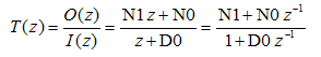
The difference equation representing this transfer function is:

For example, if N1, N0, and D0 have been set to 0, 0.1, and -0.99, respectively, the resulting first-order discrete filter will have a DC gain of 10.0, a pole located at z=0.99, and no zero.
The parameters required for the discrete filter can be found in the device documentation.
Second-Order Discrete Filter
Device Operation:
The transfer function in the z-domain for the Second-Order discrete filter is:
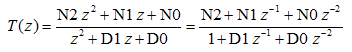
The difference equation representing this transfer function is:
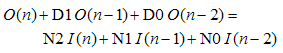
A two-pole discrete filter without any zero can be achieved with N1 and N2 both set to zero. If N2 is set to zero but N1 is non-zero, a two-pole discrete filter with a single zero is realized. If N2 is non-zero, then a two-pole two-zero discrete filter is realized.
The parameters required for the discrete filter can be found in the device documentation.
Analog to Digital Converter
Device Operation:
This is a 1-32 bit analog to digital converter. The operation of this device is illustrated by the following diagrams:
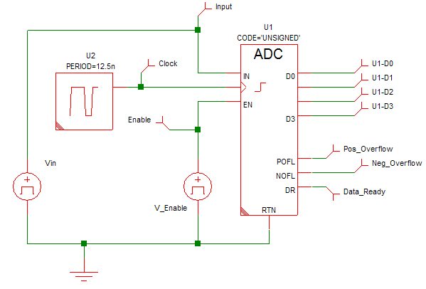
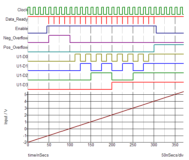
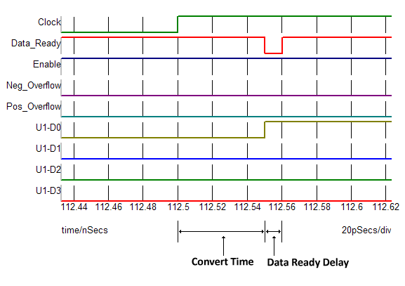
Conversion Timing:
The ADC starts the conversion at the rising or falling edge of the clock, depending on the selected value of the Trigger Condition. The sampling of the analog input signal begins at this point. The sampling of the input is complete after an interval of Sample delay. The output data changes in response to this, Convert Time seconds after the clock trigger event. At the same time that the output initially changes, the Data ready output goes low (inactive) then high again after a delay equal to Data ready delay. It is possible to start a new conversion before the previous conversion is complete provided it is started later than Minimum clock width seconds after the previous conversion was started. Minimum clock width must always be less than Convert Time. If the Minimum clock width specification is violated, the conversion will not start.
Analog to Digital Converter w/ Adjustable Voltage Reference
Device Operation:
This is a 1-32 bit analog to digital converter. The operation of this device for the most part identical to the Analog to Digital Converter described above. As shown in this figure , the major difference is that the range and offset of this device is controlled by the voltage on the analog reference pin VREF.
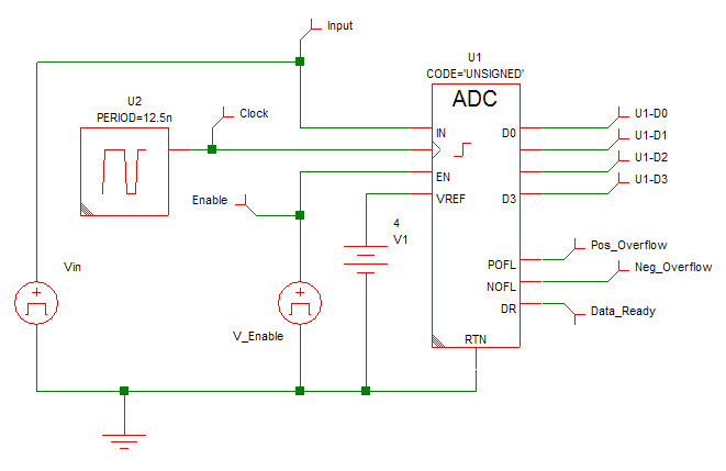
Input Range and Offset:
This ADC has an Analog Reference that determines the Input Voltage Range and the Input Voltage Offset based on the value of the analog voltage present between the VREF and RTN pins. The voltage at the VREF pin must always be positive and greater than zero. The Input Voltage Range is equal to the voltage between the VREF and RTN pins while the Input Voltage Offset is equal to 1/2 of the Input Voltage Range.
PID Discrete Filter
Device Operation:
The transfer function for an analog PID filter is:
where the A in the three coefficients KPA, KIA, and KDA are used to signify that these are the coefficients associated with Eq. (1), which is defined for the analog PID filter.
Since (1) has two zeroes and one pole, there are more zeroes than poles, resulting in an improper transfer function / filter. A pole is sometimes added to the derivative term to limit the bandwidth at higher frequencies. One form for such a PID filter with a pole added for the derivative action is:
In the discrete PID filter provided, the implemented transfer function is:
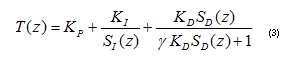
where KP, KI, and KD are coefficients entered by the user. To match the frequency response of the discrete PID filter represented by (3) to the frequency response of the analog PID filter represented by (2), a first-order approximation is to set
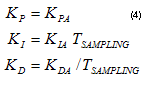
where TSAMPLING is the sampling period. If this first-order approximation is used, the frequency response for (3) will have a very good match with the frequency response for (2), as long as the poles and zeroes of (3) are more than two decades below the sampling frequency.
The functions SI(z) and SD(z) are transfer functions in the z-domain according to the integration and derivative methods selected, respectively. The choices for the method are "Forward-Euler," "Backward-Euler," and "Trapezoidal."
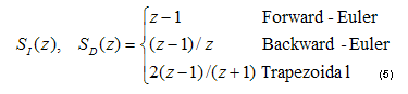
The integration and the derivative methods are sometimes referred to as the mapping / transformation in the literature. Mapping and transformation are easy and simple ways to generate discrete or digital filters with frequency responses that are approximates of the frequency response of the original s-domain analog filter. The approximation is reasonable if the poles and zeros of the original analog filter are more than two decades below the sampling frequency.
Due to the nature of (3) and (5), the discrete PID filter has two poles in the z-domain, one from the integration term, and one from the derivative term. The pole from the integration term is always located at z=1 and the pole due to the derivative term is located at:
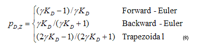
Since the location of this pole should not yield unstable responses, at the very minimum, the restraint on PD,Z is:
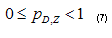
From (6) and (7), the restriction placed on the product YKD is:
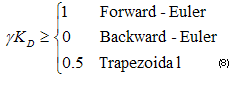
Once the value of PD,Z is set, Y can be computed from (6). The corresponding pole location in the s-domain for the pole PD,Z in the z-domain is:
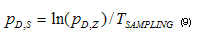
If PD,Z is set to 0.5, the corresponding pole in the s-domain would have a corner frequency of about 0.11 of the sampling frequency.
If there are already extra low-pass filter(s) along the path of feedback, it may be desirable not to introduce the extra pole associated with the derivative term in the discrete PID filter described here. While it is not exactly the same as removing the extra pole, placing PD,Z at z=0.0, the center of the origin of the complex plane, has almost the same net effect. Such a pole will have no effect on the magnitude of the derivative term, but it will introduce a phase delay to the derivative term. Such a phase delay is minimal until the signal of interest is at or above one-tenth of the sampling frequency.
If the poles and zeros of the original analog PID filter are well below the sampling frequency, then the three integration methods yield essentially the same result and the three derivative methods yield essentially the same result. The three methods were provided as a convenience if the user is using one of the three mappings or transformations as a quick way to implement a discrete PID filter when the desired analog PID transfer function has been established.
In addition, if one is using one of the three mappings, or transformations, the derivative method should be set to the same as the integration method. The two methods are allowed to be different here in case the user does not come from the point of view of mapping or transformation, but from the point of view of how to implement the integration and how to derive the derivative from the input samples.
The parameters required for the discrete filter can be found in the device documentation.