» DVM Test Report Overview
| General | |
| Schematic | 6.3_LTC3406B - DVM ADVANCED.sxsch |
| Testplan | dvm_advanced.testplan |
| Original Testplan Filename | 6.4.2_promotegraph.testplan |
| Date / Time | 2013-04-24 9:48:54 AM |
| Report Directory | DVM_REPORTS\2013-04-24-9_48_54_AM |
| Log File | dvm_advanced.log |
| # of Tests Run | 2 of 2 (2 of 2 Run, 1 Passed, 1 Failed, 0 Ran with Warnings, 0 Skipped) |
| Total Time | 16s |
| Design Specifications | |
| Circuit Name | LTC3406B |
| Description | Synchronous Buck |
| Input 1 | 5.000 V (4.5 V to 5.5 V) |
| Output 1 | 1.505 V (±5%) @ 1.5 A |
| Switching Frequency | 955kHz |
| Excel-compatible Results | |
| Scalar Results | dvm_advanced_table_scalars.txt |
| Spec Results | dvm_advanced_table_specs.txt |
| Overview Graphs | |
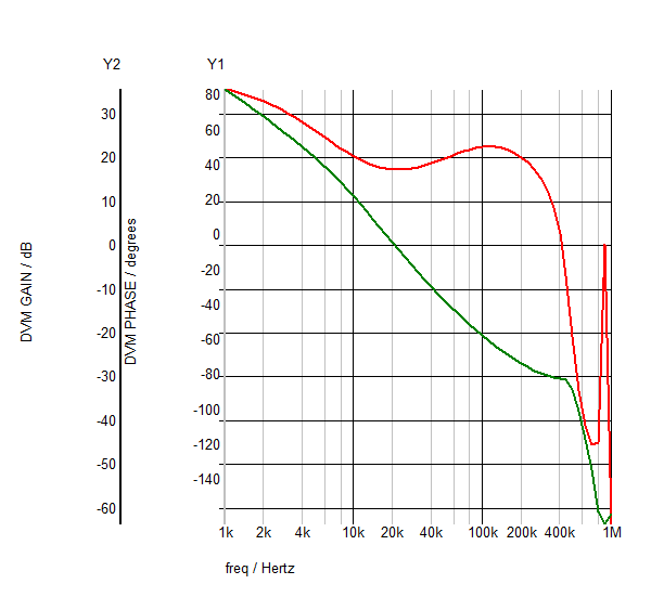 Bode Plot Nominal Vout
GAIN
PHASE
|
|
| SXGPH File | simplis_ac25_1164.sxgph |
| Source Test | VOUT=1.505V|Bode Plot|Vin Nominal|50% Load |
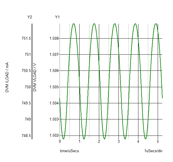 LOAD
VLOAD
ILOAD
|
|
| SXGPH File | simplis_pop25_1147.sxgph |
| Source Test | VOUT=1.505V|Bode Plot|Vin Nominal|50% Load |
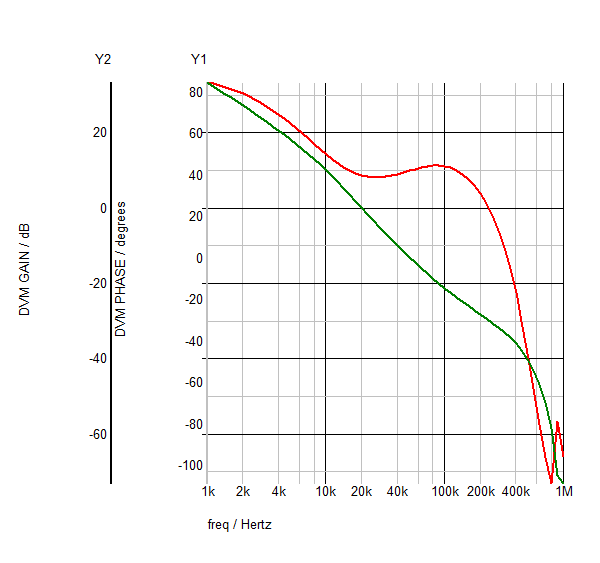 Bode Plot
GAIN
PHASE
|
|
| SXGPH File | simplis_ac26_1211.sxgph |
| Source Test | VOUT=0.6V|Bode Plot|Vin Maximum|50% Load |
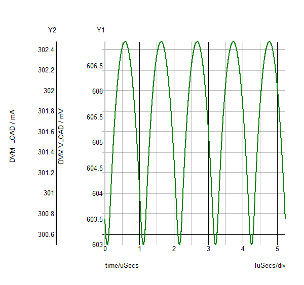 LOAD
VLOAD
ILOAD
|
|
| SXGPH File | simplis_pop26_1194.sxgph |
| Source Test | VOUT=0.6V|Bode Plot|Vin Maximum|50% Load |
| Test 1 of 2 | top ^ |
| Test Label | VOUT=1.505V|Bode Plot|Vin Nominal|50% Load |
| Simulator | simplis |
| Test Report | VOUT=1.505V\Bode Plot\Vin Nominal\50% Load\report.txt.html |
| Status | PASS |
| Test Time | 7s |
| Test 2 of 2 | top ^ |
| Test Label | VOUT=0.6V|Bode Plot|Vin Maximum|50% Load |
| Simulator | simplis |
| Test Report | VOUT=0.6V\Bode Plot\Vin Maximum\50% Load\report.txt.html |
| Status | FAIL |
| Test Time | 6s |