SIMPLIS Parts
SIMPLIS Parts
|
The Switched Voltage-Controlled Voltage Source (VCVS) models the passing of an analog voltage from input to output with unity gain. The block uses an ON/OFF control where:
VOUT = VSENSE (the input) when the control signal is in the ON state.
VOUT = RTN (ground) when the control signal is in the OFF state.
The control signal is referenced to the RTN pin.
The Logic parameter sets the control state logic. The two choices are:
POS - A CNTL voltage greater than Threshold + 1/2 Hysteresis turns on the VCVS and the output voltage equals the input voltage.
NEG - A CNTL voltage less than Threshold - 1/2 Hysteresis turns on the VCVS and the output voltage equals the input voltage.
Most users implement this function with two simple switches connected in a totem-pole configuration where VSENSE is the input voltage and VOUT is the output voltage.
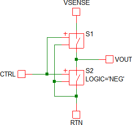
Because the SIMPLIS simple switches S1 and S2 have finite ON and OFF resistances, the totem-control configuration will always have numeric inaccuracies. These inaccuracies are caused by the inherent resistive divider network formed by the switch resistances. More importantly, the totem-pole switch implementation can slow down your simulation if a small capacitive load is applied to the output. This is due to the R-C time constant formed by the switch on resistance and the capacitive load.
In contrast to the totem-pole switch circuit, this block was designed to eliminate the numeric inaccuracies caused by the voltage divider, and doesn't suffer from slow simulations with capacitive loads. You should always use this block instead of a totem-pole switch configuration since this block is speed-optimized for SIMPLIS simulations and does not exhibit the numeric inaccuracy inherent to the totem-pole switch configuration.
In this Topic Hide
Model Name: |
Switched Voltage-Controlled Voltage Source |
|
Simulator: |
|
This device is compatible with the SIMPLIS simulator. |
Parts Selector |
Controlled Sources | Voltage-Controlled Voltage Source with turn-on/turn-off |
|
Symbol Library: |
SIMPLIS_BB.sxslb |
|
Model File: |
SIMPLIS_cntl_parts_BB.lb |
|
Subcircuit Name: |
SIMPLIS_SWITCH_VCVS_BB |
|
Symbols: |
|
|
Multiple Selections: |
Multiple devices can be selected and edited simultaneously. |
|
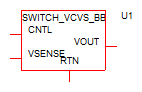
The following table describes the pins on the Switched VCVS symbol.
Pin_Name |
I/O |
Function |
Description |
CNTL |
I |
On/Off control voltage |
The threshold voltage, hysteresis, and logic of the control voltage are set in the input dialog box described in Editing_the_Switched_VCVS. |
VSENSE |
I |
Input voltage for VCVS |
The input voltage for the VCVS |
RTN |
|
Circuit return for this VCVS |
The ground reference for this circuit |
VOUT |
O |
Output Voltage for VCVS |
VOUT = VSENSE when the CNTL signal is in the ON state. VOUT = 0 when the CNTL signal is in the OFF state. The initial condition can be set to either ON or OFF. |
To configure the Switched VCVS, follow these steps:
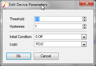
| Label | Parameter Description |
Threshold |
The threshold voltage of the CNTL signal; default is 2.5. |
Hysteresis |
The hysteresis of the CNTL signal; default is 1. |
Initial Condition |
Initial condition of the CNTL signal: default is 0 Off. |
Logic |
The logic of the CNTL signal, which can be set to positive or negative; default is 'POS'. |
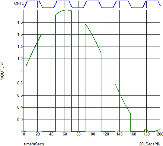
The test circuit used to generate the waveform examples in the next section can be downloaded here: simplis_071_switched_vcvs.sxsch.

The waveform below is the test circuit showing a sinusoidal VSENSE waveform and an asynchronous CNTL waveform.
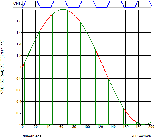
The following waveform is for the test circuit with VSENSE hidden.
© 2015 simplistechnologies.com | All Rights Reserved