SIMPLIS Parts
SIMPLIS Parts
|
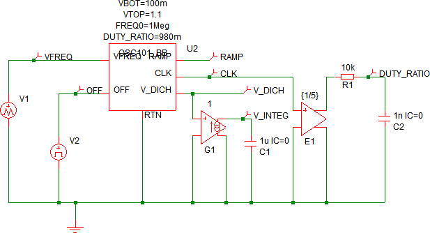
The Voltage Controlled Oscillator w/ Programmable Duty Cycle models a VCO with programmable ramp peak and valley voltages and a voltage-to-frequency gain. This block is speed-optimized for SIMPLIS simulations and can be used as a fixed frequency oscillator by connecting a constant DC voltage source to the frequency pin. This oscillator includes an ON/OFF control pin and outputs commonly used signals that include the following:
For a VCO with a 50% duty cycle, see the Voltage-Controlled Oscillator w/ 50% Duty Cycle topic.
In this Topic Hide
Model Name: |
Basic Voltage-Controlled Oscillator |
|
Simulator: |
|
This device is compatible with the SIMPLIS simulator. |
Parts Selector |
Analog Functions | Timing and Oscillators | Basic Voltage-Controlled Oscillator (No sync.) |
|
Symbol Library: |
SIMPLIS_BB.sxslb |
|
Model File: |
SIMPLIS_cntl_parts_BB.lb |
|
Subcircuit Name: |
SIMPLIS_OSC101_BB |
|
Symbols: |
|
|
Multiple Selections: |
Multiple devices can be selected and edited simultaneously. |
|
The following table describes the pins on the VCO symbol.
Pin_Name |
I/O |
Function |
Description |
VFREQ |
I |
Input voltage that controls the clock frequency. |
\[ f_{CLK} = VFREQ \times f_0 \] |
OFF |
I |
On/Off control voltage for the oscillator |
Oscillator runs when the OFF voltage signal is less than 2.0V.
|
RTN |
|
The circuit return for the VCO |
The ground reference for this circuit |
RAMP |
O |
Saw tooth ramp voltage output |
This output allows you to probe the internal oscillator ramp voltage.
|
CLK |
O |
Digital logic output Logic 0 => CLK = 0V |
The clock frequency is controlled by the VFREQ input. The clock parameters are set in the input dialog box described in Editing_the_VCO.
|
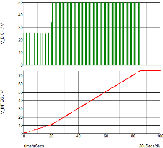
V_DICH |
O |
V_DICH output voltage |
V_DICH provides output voltage signal. When this output is connected as shown in the schematic example below, the V_INTEG signal is proportional to the number of clock cycles. |
To configure the VCO, follow these steps:
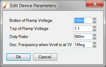
| Label | Parameter Description |
Bottom of Ramp Voltage |
The valley of the ramp voltage |
Top of Ramp Voltage |
The peak of the ramp voltage |
Duty Ratio |
The clock and ramp duty cycle |
Osc. Frequency when Vcntl is at 1V |
The frequency when VFREQ = 1.0 |
The test circuit used to generate the waveform examples in the next section can be downloaded here: simplis_070_vco_programmable_duty.
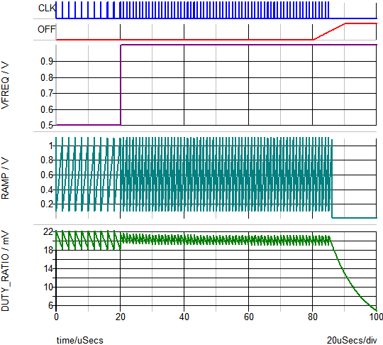
The following image shows the frequency change event zoomed in.
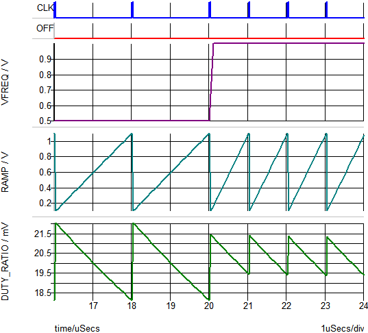
Note: A test circuit is added to the output CLK to create an output voltage DUTY-RATIO proportional to the duty ratio of the CLK signal.
The waveform below shows the integrator output proportional to the number of clock cycles. The V_INTEG voltage increases 1V for every oscillator cycle.
© 2015 simplistechnologies.com | All Rights Reserved

