Reduce Hardware Iterations with SIMPLIS
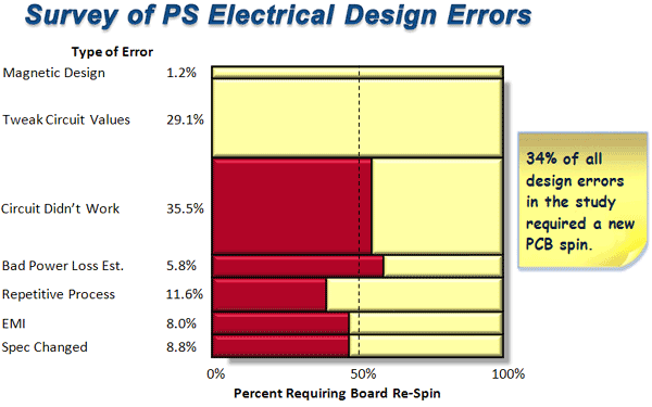
The following data are the result of in-depth studies of five large design organizations at three major manufacturers of custom and standard power supplies.

- All engineering change orders during each study period (6 to 9 months) were evaluated to determine the nature of each design change and whether or not correcting the design flaw required a new Printed Circuit Board (PCB) layout (in red).
- The most painful design changes are those that require an additional hardware iteration. As shown in green in the next slide, more than 50% of these design errors could have been detected with simulation prior to the PCB layout.
